Manufacturing method of 3D memory device

A manufacturing method and technology of storage devices, applied in the field of memory, capable of solving problems such as current leakage and uneven epitaxial layer

Active Publication Date: 2019-01-18
YANGTZE MEMORY TECH CO LTD
View PDF4 Cites 17 Cited by
  • Summary
  • Abstract
  • Description
  • Claims
  • Application Information

AI Technical Summary

Problems solved by technology

[0005] In view of the above problems, the object of the present invention is to provide a method for manufacturing a 3D memory device, which can solve the problems of uneven epitaxial layer and current leakage due to the formation of the epitaxial layer in the auxiliary region.

Method used


Image

  • Manufacturing method of 3D memory device
  • Manufacturing method of 3D memory device
  • Manufacturing method of 3D memory device

Examples


Embodiment Construction

[0043] Various embodiments of the invention will be described in more detail below with reference to the accompanying drawings. In the various drawings, the same elements are denoted by the same or similar reference numerals. For the sake of clarity, various parts in the drawings have not been drawn to scale.

[0044] The specific implementation manners of the present invention will be further described in detail below in conjunction with the accompanying drawings and embodiments.

[0045] "Above" described in the present invention refers to being located above the plane of the substrate, which may refer to direct contact between materials, or may be arranged at intervals.

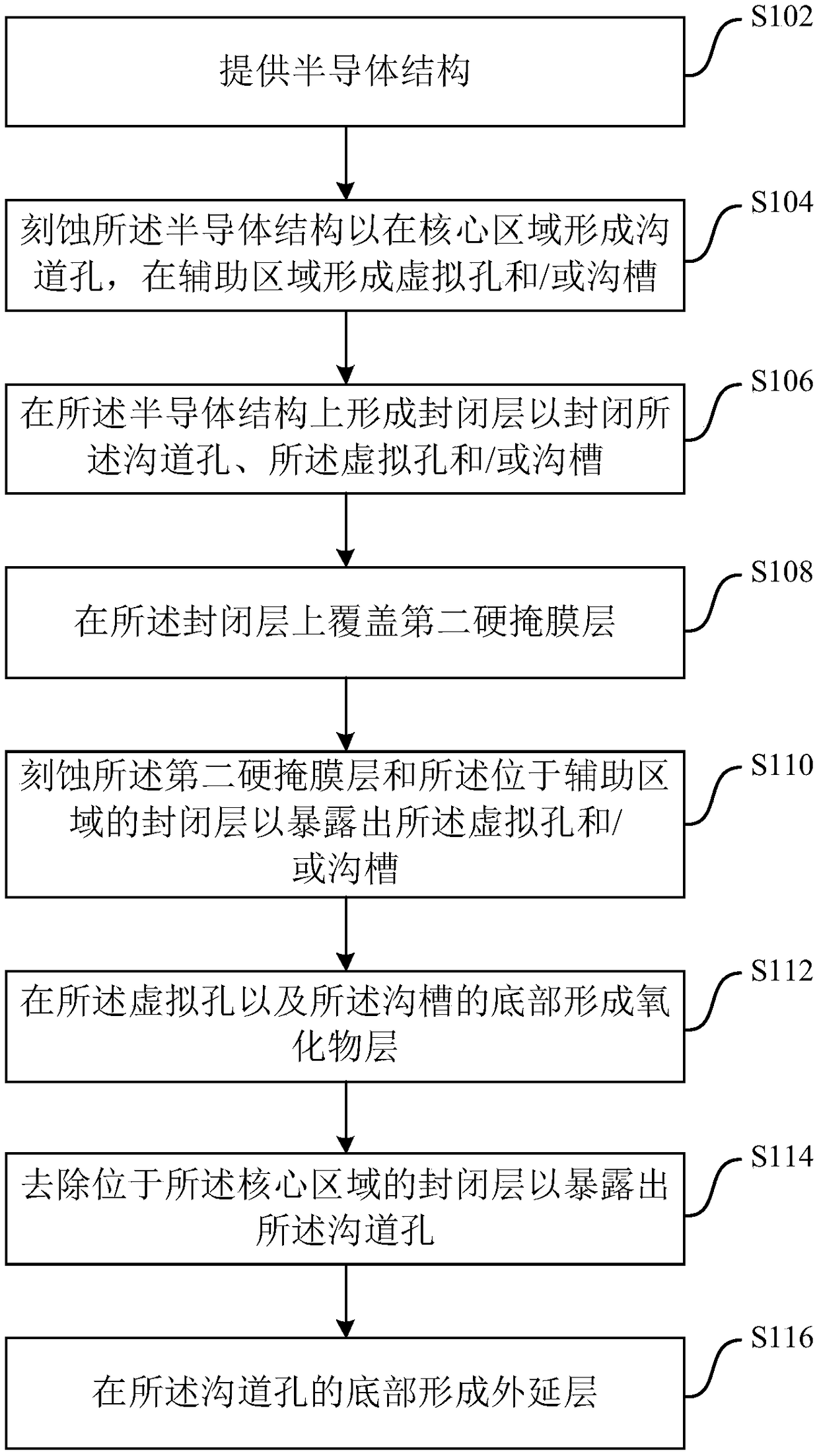
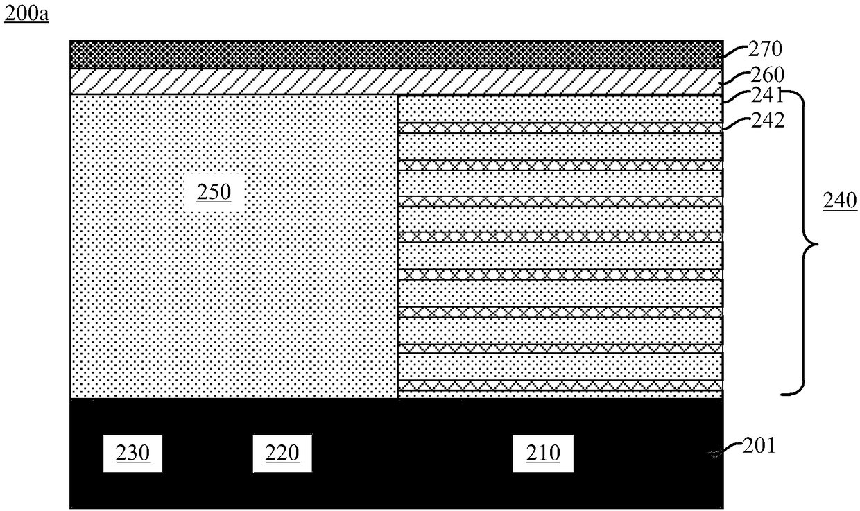
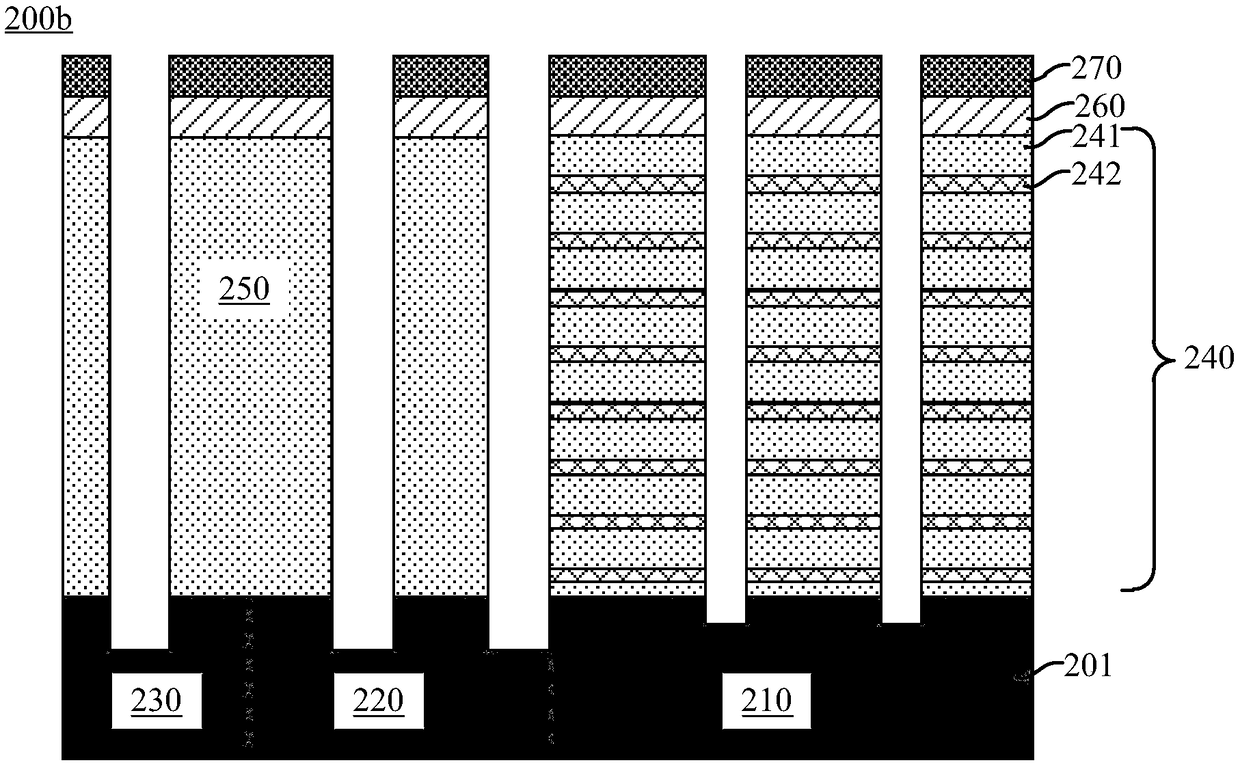
[0046] figure 1 A flowchart showing a method for manufacturing a 3D storage device according to a first embodiment of the present invention. Figure 2A - FIG. 2M shows cross-sectional views of various stages of a method of manufacturing a 3D memory device according to a first embodiment of the present i...


PUM


Abstract

A manufacturing method of a 3D memory device is disclosed, comprising: providing a semiconductor structure including a core region and an auxiliary region; etching the semiconductor structure to formchannel holes in the core region and forming dummy holes and / or trenches in the auxiliary region; forming an oxide layer at the bottom of the dummy hole and the trench; forming an epitaxial layer at the bottom of the channel hole. an embodiment of the present invention forms an oxide layer in a virtual hole and / or a trench in an auxiliary region, and forms an epitaxial layer in a channel hole in acore region, thereby solving problems such as uneven epitaxial layer and current leakage caused by forming an epitaxial layer in the auxiliary region.

Description

technical field [0001] The invention relates to the technical field of memory, in particular to a 3D memory device and a manufacturing method thereof. Background technique [0002] The improvement of the storage density of the memory device is closely related to the progress of the semiconductor manufacturing process. As the feature size of the semiconductor manufacturing process becomes smaller and smaller, the storage density of the memory device becomes higher and higher. In order to further increase storage density, memory devices with a three-dimensional structure (ie, 3D memory devices) have been developed. A 3D memory device includes a plurality of memory cells stacked in a vertical direction, which can double the integration level on a wafer per unit area and reduce the cost. [0003] A 3D memory device includes a core region forming a memory cell and an auxiliary region forming a peripheral structure. In 3D memory devices, such as 3D NAND flash memory, it is nece...

Claims


Application Information

Patent Timeline
Patent Type & Authority Applications(China)
IPC IPC(8): H01L27/11524H01L27/11529H01L27/11531H01L27/11551H01L27/1157H01L27/11573H01L27/11578
CPCH10B41/35H10B41/41H10B41/42H10B41/20H10B43/35H10B43/40H10B43/20
Inventor 肖莉红
Owner YANGTZE MEMORY TECH CO LTD
Why Eureka
Try Eureka