Array substrate and manufacturing method thereof, display panel and display device

A technology for an array substrate and a base substrate is applied in the fields of an array substrate and a manufacturing method thereof, a display panel and a display device, and can solve problems such as poor wire breakage and the like

Active Publication Date: 2019-01-18
BOE TECH GRP CO LTD
View PDF4 Cites 18 Cited by
  • Summary
  • Abstract
  • Description
  • Claims
  • Application Information

AI Technical Summary

Problems solved by technology

[0003] Embodiments of the present invention provide an array substrate and a manufacturing method thereof

Method used


Image

  • Array substrate and manufacturing method thereof, display panel and display device
  • Array substrate and manufacturing method thereof, display panel and display device
  • Array substrate and manufacturing method thereof, display panel and display device

Examples


Embodiment Construction

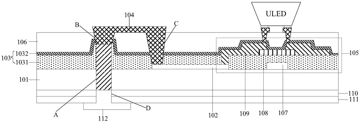
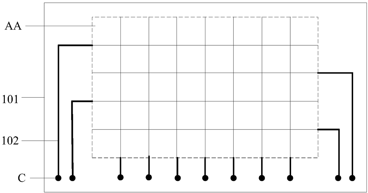
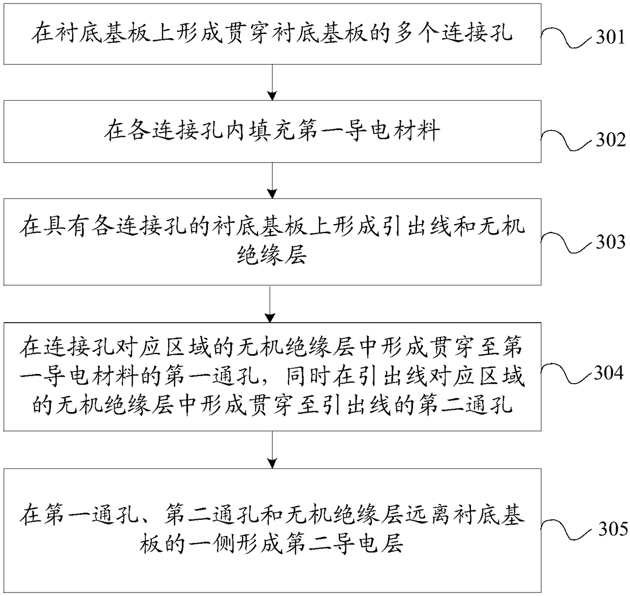
[0036] The specific implementation manners of the array substrate and the manufacturing method thereof, the display panel, and the display device provided by the embodiments of the present invention will be described in detail below with reference to the accompanying drawings. It should be noted that the embodiments described in this specification are only some of the embodiments of the present invention, not all of them; and in the case of no conflict, the embodiments in this application and the features in the embodiments can be combined with each other; In addition, based on the embodiments of the present invention, all other embodiments obtained by persons of ordinary skill in the art without making creative efforts belong to the protection scope of the present invention.

[0037] The shape and size of each film layer in the drawings do not reflect their real proportions in the array substrate, but are only intended to schematically illustrate the content of the present inv...


PUM


Abstract

The invention discloses an array substrate and a manufacturing method thereof, a display panel, a display device. the array substrate comprises a substrate, a lead-out wire and an inorganic insulatinglayer located on one side of the substrate; The substrate has a plurality of connection holes penetrating the substrate and filled with a first conductive material. The inorganic insulating layer isprovided with a first through hole and a second through hole, wherein the first through hole penetrates into the first conductive material and the second through hole penetrates into the lead wire; The second conductive layer is located at a side of the first via hole, the second via hole and the inorganic insulating layer away from the substrate so that the first conductive material and the leadwire are electrically connected through the second conductive layer. Since the electrical connection between the lead wire and the first conductive material can be realized by punching the first through hole and the second through hole after the high-temperature process of manufacturing the lead wire and the inorganic insulating layer is finished, the connection between the signal wire and the traces of the integrated circuit chip is effectively ensured, and the wire breakage defect caused by the expansion of the first conductive material such as copper is solved.

Description

technical field [0001] The present invention relates to the field of display technology, in particular to an array substrate and a manufacturing method thereof, a display panel, and a display device. Background technique [0002] Through Glass Via (TGV for short) technology is a key technology for manufacturing three-dimensional integrated circuits. Generally, the TGV technology uses a laser to open a through hole with a width of tens to hundreds of microns on glass with a thickness of several hundred microns, and then fills the through hole with copper (Cu) to connect electronic components. Contents of the invention [0003] Embodiments of the present invention provide an array substrate and a manufacturing method thereof, a display panel and a display device, so as to solve the problem of poor disconnection caused by Cu expansion. [0004] Therefore, an array substrate provided by an embodiment of the present invention includes a base substrate, a lead wire located on o...

Claims


Application Information

Patent Timeline
IPC IPC(8): H01L27/12H01L21/77
CPCH01L27/1244H01L27/1259H01L27/124H01L23/481H01L23/482H01L23/5226H01L23/53228H01L27/1262H01L33/382H01L33/387
Inventor 顾仁权姚琪黎午升李东升吴慧利李士佩尹东升贺芳岳阳
Owner BOE TECH GRP CO LTD
Why Eureka
Try Eureka