

Batch transfer device and transfer method for microchip
A transfer device and chip technology, applied in transportation and packaging, conveyor objects, furnaces, etc., can solve problems such as efficiency, yield and transfer accuracy, and practical application obstacles.
- Summary
- Abstract
- Description
- Claims
- Application Information
AI Technical Summary
Problems solved by technology
Method used
Image

Examples
Embodiment 1
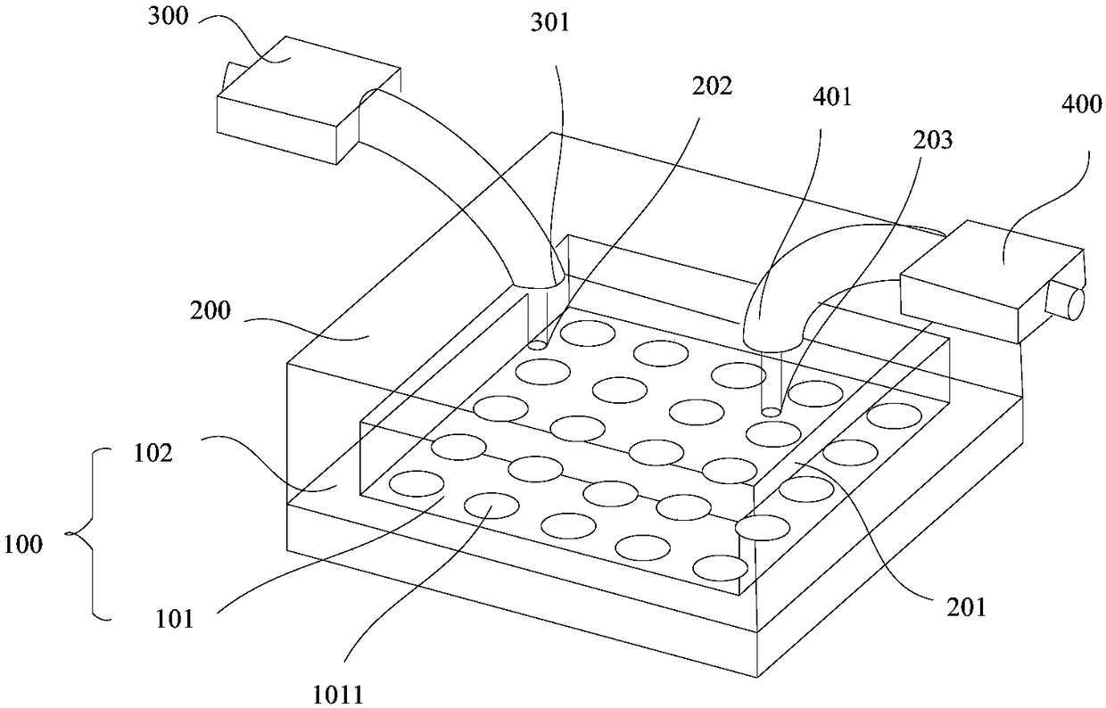
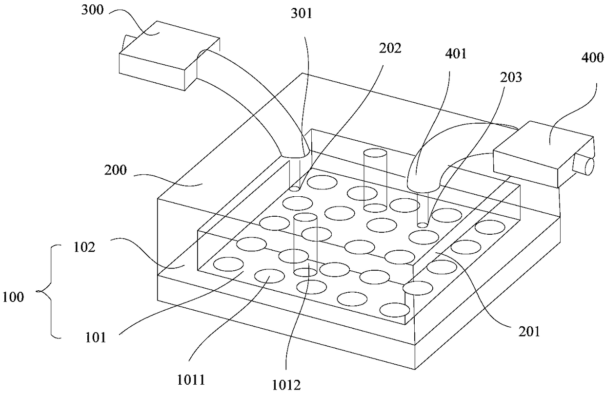
[0036] Embodiments of the present invention provide a batch transfer device for microchips. see figure 1 , the batch transfer device for microchips specifically includes: a loading mold 100, the loading mold 100 includes a loading area 101 and a non-loading area 102 located at the edge of the loading area 101; a plurality of chip suction holes arranged in an array formed on the loading area 101 1011; the outer cover 200 formed on the non-loading area 102, the cavity 201 is formed between the outer cover 200 and the loading mold 100; the air suction holes 202 and the inflation holes 203 formed on the outer cover 200; The input port 301 is sealedly connected to the air suction hole 202 for extracting the gas in the chamber 201 ; the inflator 400 , the output port 401 of the inflator 400 is sealedly connected to the inflation hole 203 for inflating the chamber 201 .
[0037] Through high-precision equipment, a large number of microchips are arranged on the target substrate or ci...
Embodiment 2
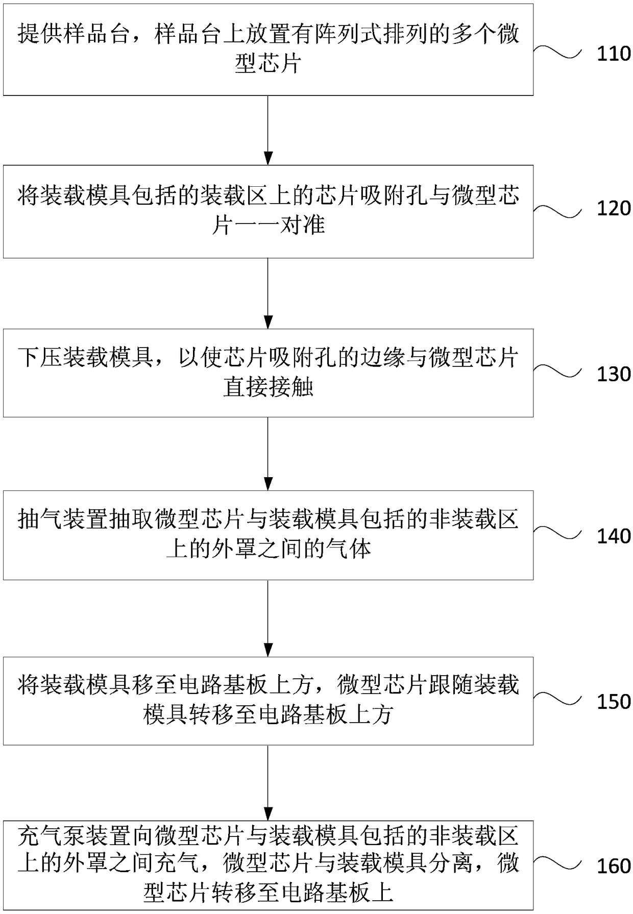
[0048] Based on the same concept as the above-mentioned embodiments, the embodiments of the present invention provide a batch transfer method for microchips, see image 3 , the method steps are as follows:
[0049] Step 110 , providing a sample stage on which a plurality of microchips arranged in an array are placed.
[0050] see Figure 4 , a sample stage 500 is provided, and a plurality of microchips 501 arranged in an array are placed on the sample stage 500 .
[0051] In this embodiment, the micro chip is exemplarily a micro light emitting diode chip. The specific preparation method of the miniature light-emitting diode chip can use metal organic chemical vapor deposition, deposit a gallium nitride GaN epitaxial layer on a clean sapphire substrate, and the epitaxial layer includes but is not limited to n-type GaN epitaxial layer, multiple quantum well layer, p-type GaN layer The epitaxial layer is made by lithography, cleaning, etching, electrode deposition and other ch...
PUM
 Abstract
Description
Claims
Application Information