A method for performing solder resistance and plugging on holes

A technology of plugging and solder resistance, applied in the direction of electrical components, printed circuit manufacturing, printed circuits, etc., can solve problems such as exposed copper, redness of the hole, fullness of cracks, etc., to solve various defects and increase window opening The effect of increasing size and plumpness

Inactive Publication Date: 2019-01-22
珠海杰赛科技有限公司 +1
View PDF5 Cites 1 Cited by
  • Summary
  • Abstract
  • Description
  • Claims
  • Application Information

AI Technical Summary

Problems solved by technology

The process is as follows: pre-treatment --- plug hole --- printed solder mask --- pre-baking --- alignment --- exposure --- development --- inspection board --- post-baking, conventional solder mask plug hole After the circuit pattern is made, the solder mask plug hole and the printed solder mask

Method used


Image

  • A method for performing solder resistance and plugging on holes
  • A method for performing solder resistance and plugging on holes
  • A method for performing solder resistance and plugging on holes

Examples


Embodiment Construction

[0015] In order to make the object, technical solution and advantages of the present invention clearer, the present invention will be further described in detail in conjunction with the accompanying drawings and embodiments. It should be understood that the specific embodiments described here are only used to explain the present invention, and are not limited to the present invention.

[0016] The present invention is described in further detail below in conjunction with accompanying drawing embodiment:

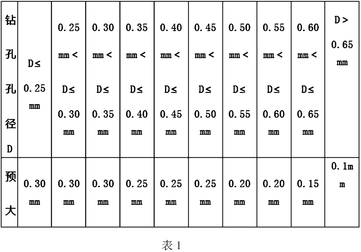
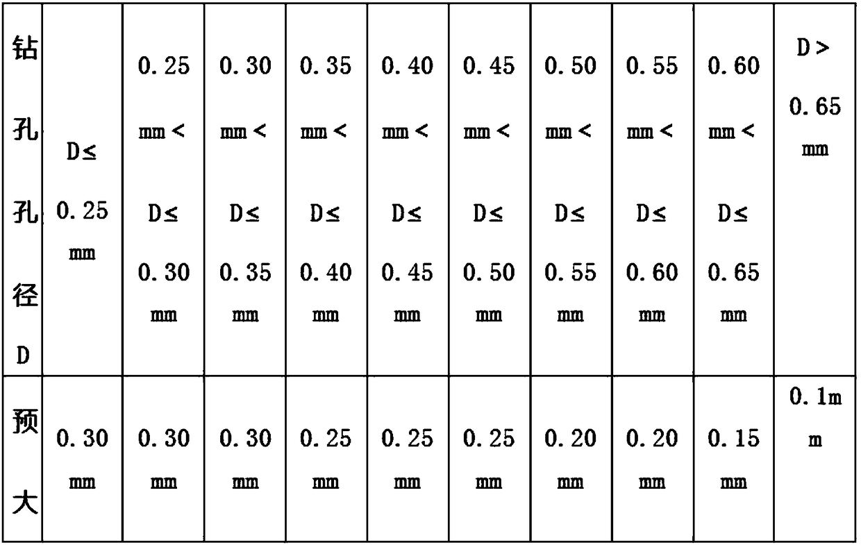
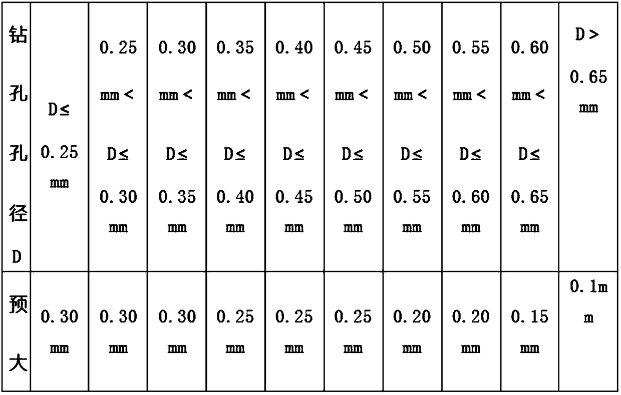
[0017] A method for plugging holes with solder resistance, comprising the following steps in turn: metallization of PCB board holes → micro-etched PCB boards → solder masking for plug holes → making aluminum mesh for plug holes → installing mesh → aligning → first piece production → Parameter adjustment→mass production→pre-baking→exposure→baking→solder mask grinding, the process of plugging the solder mask holes is placed after the metallization process of the PCB board holes...


PUM

PropertyMeasurementUnit
Apertureaaaaaaaaaa
Apertureaaaaaaaaaa
Apertureaaaaaaaaaa

Abstract

A method for performing solder resistance and plugging on holes comprises the following steps in turn: metallization of PCB plate holes,micro-etched wire of PCB plates,solder resistance of collector plug holes,manufacture of plug hole aluminum meshes,mesh loading ,alignment,first article manufacture, parameter adjustment ,batch production,pre-drying ,exposure,baking, solder resistance grinding. The invention improves the traditional production flow, The method for performing solder resistance and plugging on holes is used., solder resistance and plugging on holes are carried out after the holes are metallized, which replaces the traditional plug holes after pattern making enlarges the window size of aluminum sheet, solves many defects brought by the traditional making, increases the plumpness of solder plug hole to more than 70%, and improves the finished product rate.

Description

【Technical field】 [0001] The invention relates to the field of PCB board manufacture, in particular to a method for plugging holes with solder resistance. 【Background technique】 [0002] At present, the manufacturing method of PCB internal solder resist plug holes is mainly to perform plug hole treatment before printing solder resist, and then perform pre-baking and exposure processing. The process is as follows: pre-treatment --- plug hole --- printed solder mask --- pre-baking --- alignment --- exposure --- development --- inspection board --- post-baking, conventional solder mask plug hole After the circuit pattern is made, the solder mask plug hole and the printed solder mask are used. With this scheme, the quality of the plug hole is poor, and defects such as redness of the hole, exposed copper, cracks, and low fullness often appear. The saturation is only low. It can be controlled at more than 60%, and a variety of defects lead to a high damage rate of the PCB board. ...

Claims


Application Information

Patent Timeline
IPC IPC(8): H05K3/00
CPCH05K3/0094
Inventor 彭玉峰胡伦红李超谋
Owner 珠海杰赛科技有限公司
Why Eureka
Try Eureka