Hall device applied to three-dimensional Hall sensor, and method thereof

A Hall sensor and Hall device technology, applied in the direction of the magnitude/direction of the magnetic field, instruments, three-component magnetometer, etc., can solve the problems of increasing the area of ​​the Hall device, asymmetric structure, high offset voltage, etc., to eliminate Effects of offset voltage, reduced layout area, and low initial offset

Pending Publication Date: 2019-01-25
FUZHOU UNIV
View PDF5 Cites 3 Cited by
  • Summary
  • Abstract
  • Description
  • Claims
  • Application Information

AI Technical Summary

Problems solved by technology

The vertical Hall device is used to detect the magnetic field parallel to the surface of the chip. Therefore, two sets of Hall devices are required, corresponding to the detection of the X-axis and Y-axis magnetic fields. Common structures include four-hole, five-hole and six-hole structures. Including a set of bias electrodes and a set of Hall electrodes, the electrodes are distributed parallel to the surface of the structure, but the well depth of the vertical Hall device is shallow in the standard process, and the sensitivity is low; in these designs, there is structural asymmetry or current path is not The disadvantage of symmetry, with a higher offset voltage
In addition, the discrete structure increases the area of ​​the Hall device in the layout

Method used


Image

  • Hall device applied to three-dimensional Hall sensor, and method thereof
  • Hall device applied to three-dimensional Hall sensor, and method thereof
  • Hall device applied to three-dimensional Hall sensor, and method thereof

Examples


Embodiment Construction

[0031] The present invention will be further described below in conjunction with the accompanying drawings and embodiments.

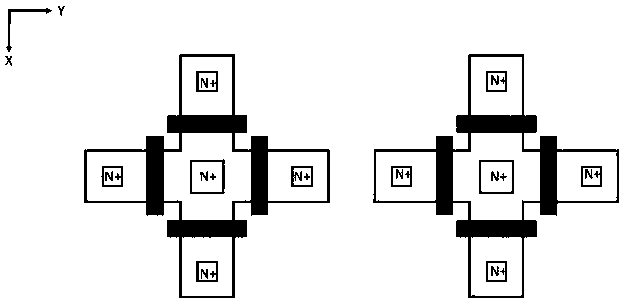
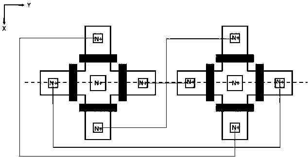
[0032] Please refer to figure 1 , the present invention provides a Hall device applied to a three-dimensional Hall sensor, the Hall device is two completely symmetrical deep N wells with a cross structure; the four ends and the center of the deep N wells with a cross structure are respectively A heavily doped N+ region layer is provided, and a highly doped P+ region layer is arranged between the four terminal heavily doped N+ region layers and the center heavily doped N+ region layer.

[0033] In an embodiment of the present invention, the Hall device is based on a silicon substrate.

[0034] In an embodiment of the present invention, the cross structure is formed by stacking two three-hole vertical Hall devices.

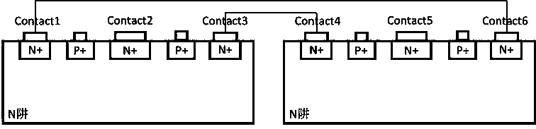
[0035] In an embodiment of the present invention, the three-hole vertical Hall device is provided with three heavily doped N+ regions on a...


PUM


Abstract

The invention relates to a Hall device applied to a three-dimensional Hall sensor. The Hall device is characterized in that the Hall device is a deep N-well of two cross structures in full symmetry, wherein four ends and the center of the N-well of the cross structures are each provided with a heavily-doped N+ region layer, and a heavily-doped P+ region layer is arranged between the central heavily-doped N+ region layer and each of the heavily-doped N+ region layers at the four end points. The Hall device is prepared by adopting a high-voltage CMOS process, has the deep N-well, improves the sensitivity of the device, can detect the magnetic induction intensity in three axial directions in a time-sharing manner under the control of the timing sequence, and greatly reduces the layout area when compared to a discrete type three-dimensional Hall device.

Description

technical field [0001] The invention relates to a Hall device applied to a three-dimensional Hall sensor and a method thereof. Background technique [0002] At present, the three-dimensional Hall sensor uses the front-end Hall device to complete the magnetoelectric conversion function. The structure is mainly discrete, including a set of horizontal Hall devices and two groups of vertical Hall devices. The horizontal Hall device is mainly a cross-shaped structure, which is used to detect the magnetic field perpendicular to the surface of the chip. A bias voltage is applied at both ends of the symmetry, and a current flows through the device. When there is a magnetic field, the carriers are subjected to the Lorentz force. The effect of the offset produces a Hall voltage at the remaining two ends. The vertical Hall device is used to detect the magnetic field parallel to the surface of the chip. Therefore, two sets of Hall devices are required, corresponding to the detection of...

Claims


Application Information

Patent Timeline
Patent Type & Authority Applications(China)
IPC IPC(8): G01R33/07G01R33/02
CPCG01R33/0206G01R33/07
Inventor 魏榕山杜宇轩刘莉莉
Owner FUZHOU UNIV
Why Eureka
Try Eureka