Display panel, manufacturing method thereof, and display device

A manufacturing method and display panel technology, applied in semiconductor/solid-state device manufacturing, electrical components, electrical solid-state devices, etc., can solve the problem of a large number of masks

Active Publication Date: 2019-01-25
BOE TECH GRP CO LTD
View PDF7 Cites 9 Cited by
  • Summary
  • Abstract
  • Description
  • Claims
  • Application Information

AI Technical Summary

Problems solved by technology

[0003] Embodiments of the present invention provide a display panel, a manufacturing method thereof, and a display device to solve the problem of a large number of masks for LTPO products in the prior art

Method used


Image

  • Display panel, manufacturing method thereof, and display device
  • Display panel, manufacturing method thereof, and display device
  • Display panel, manufacturing method thereof, and display device

Examples


Embodiment Construction

[0037] To solve the problem of a large number of masks for LTPO products in the prior art, embodiments of the present invention provide a display panel, a manufacturing method thereof, and a display device.

[0038] The specific implementation manners of the display panel provided by the embodiments of the present invention, its manufacturing method and the display device will be described in detail below with reference to the accompanying drawings. The thickness and shape of each film layer in the drawings do not reflect the real scale, and the purpose is only to illustrate the content of the present invention.

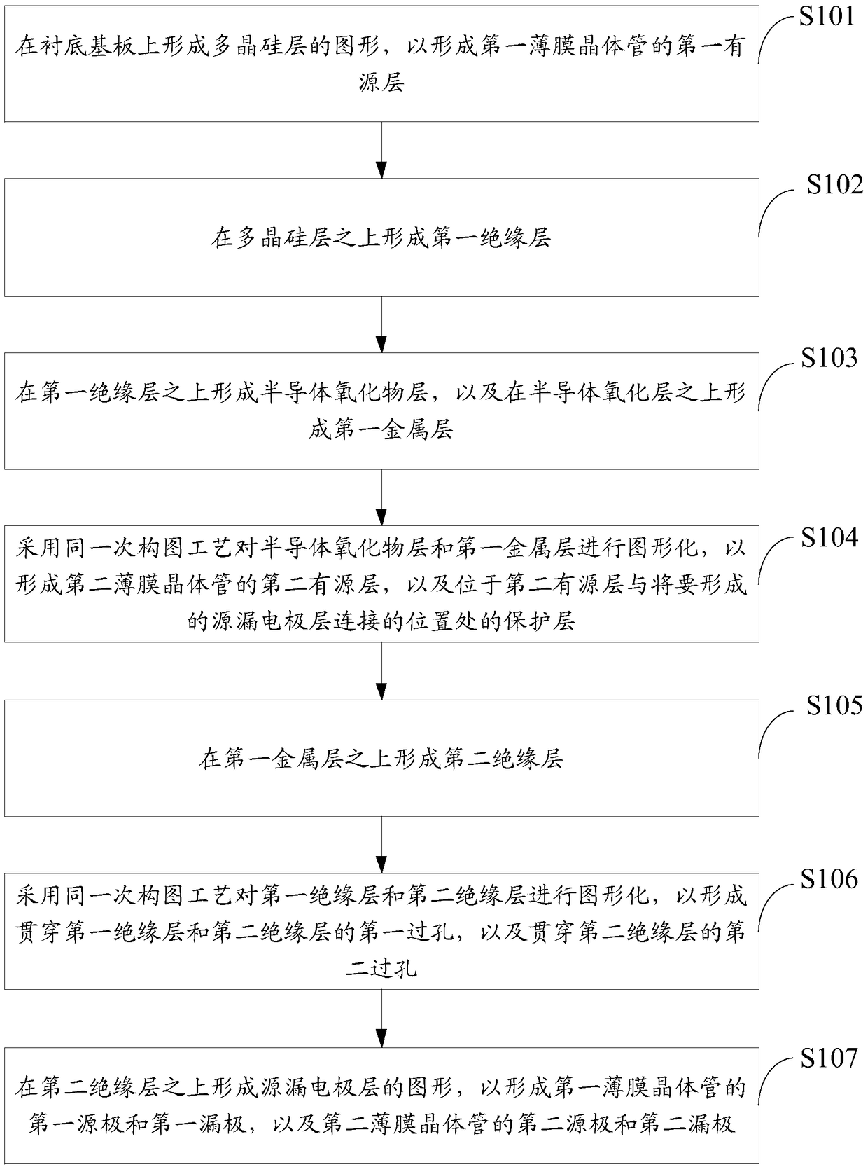
[0039] In a first aspect, an embodiment of the present invention provides a method for manufacturing a display panel, such as figure 1 shown, including:

[0040] S101, forming a pattern of a polysilicon layer on a base substrate to form a first active layer of a first thin film transistor;

[0041] S102, forming a first insulating layer on the polysilicon layer;

...


PUM


Abstract

The invention discloses a display panel, a manufacturing method and a display device thereof. The manufacturing method comprises the following steps: forming a pattern of a polysilicon layer on a substrate; Forming a first insulating layer over the polysilicon layer; Forming a semiconductor oxide layer over the first insulating layer and forming a first metal layer over the semiconductor oxide layer; patterning The semiconductor oxide layer and the first metal layer by the same patterning process; Forming a second insulating layer over the first metal layer; patterning The first insulating layer and the second insulating layer by the same patterning process; forming A pattern of source and drain electrode layers over the second insulating layer. By providing a protective layer, the secondactive layer exposed at the second via hole can be protected, so that the first via hole and the second via hole can be fabricated by the same patterning process, the primary patterning process is saved, the process stability is ensured, the number of patterning processes and the number of mask plates are reduced, and the manufacturing cost is reduced.

Description

technical field [0001] The invention relates to the field of display technology, in particular to a display panel, a manufacturing method and a display device. Background technique [0002] In recent years, two semiconductors, Low Temperature Poly-silicon (LTPS) and metal oxide (Oxide), have attracted much attention in the display industry, each with its own advantages, and they are evenly matched. LTPS has the advantages of high mobility and fast charging, and Oxide has the advantage of low leakage current. If the advantages of these two materials can be combined to form LTPO (LTPS+Oxide) products, then the user experience of display products will be greatly improved. However, the respective preparation processes of LTPS and Oxide are quite different, that is, there are problems of difficult process compatibility and process stability; moreover, the LTPS+Oxide process is relatively complicated and requires a large number of masks. , resulting in high product costs. Theref...

Claims


Application Information

Patent Timeline
Patent Type & Authority Applications(China)
IPC IPC(8): H01L21/84H01L27/12
CPCH01L27/1225H01L27/124H01L27/1288H01L27/1255H01L27/1229H01L27/127H01L27/1218
Inventor 杨维袁广才宁策卢鑫泓
Owner BOE TECH GRP CO LTD
Why Eureka
Try Eureka