Display panel and preparation method thereof, and display device

A technology for display panels and substrate substrates, applied in the fields of instruments, electrical digital data processing, electrical components, etc., can solve the problems of excessive cathode resistance, voltage drop, difficulty in further realizing ultra-thin ITD display devices, etc., to improve the voltage The effect of reducing and reducing resistance

Active Publication Date: 2019-02-01
HEFEI XINSHENG OPTOELECTRONICS TECH CO LTD +1
View PDF8 Cites 10 Cited by
  • Summary
  • Abstract
  • Description
  • Claims
  • Application Information

AI Technical Summary

Problems solved by technology

[0004] However, since the aperture ratio of OLED display devices with bottom-emitting OLED devices is limited by opaque structures such as TFT (Thin Film Transistor, thin film transistors), it is difficult for emissive OLED display devices to achieve high-resolution display requirements. Therefore, OLED display devices with top-emitting OLED devices are mostly used in the prior art
However, in the top-emitting OLED device, the light needs to be emitted from the cathode side, so the thickness of the cathode needs to be prepared thinner, resulting in excessive cathode resistance and voltage drop.
[0005] In addition, in the Integrated-touch-driver (ITD for short) technology, it is difficult to further realize the ultra-thinning of the ITD display device because touch electrodes need to be provided in the OLED display device.

Method used


Image

  • Display panel and preparation method thereof, and display device
  • Display panel and preparation method thereof, and display device
  • Display panel and preparation method thereof, and display device

Examples


Embodiment Construction

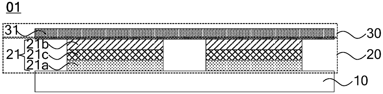
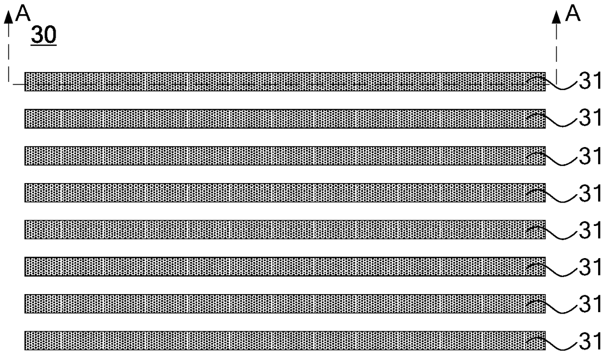
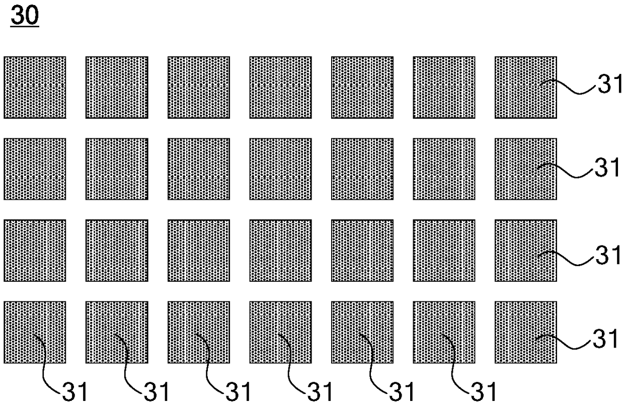
[0038] The following will clearly and completely describe the technical solutions in the embodiments of the present invention with reference to the accompanying drawings in the embodiments of the present invention. Obviously, the described embodiments are only some, not all, embodiments of the present invention. Based on the embodiments of the present invention, all other embodiments obtained by persons of ordinary skill in the art without making creative efforts belong to the protection scope of the present invention.

[0039] Hereinafter, the terms "first" and "second" are used for descriptive purposes only, and cannot be understood as indicating or implying relative importance or implicitly specifying the quantity of indicated technical features. Thus, a feature defined as "first" and "second" may explicitly or implicitly include one or more of these features. In the description of the embodiments of the present application, unless otherwise specified, "plurality" means two...


PUM


Abstract

The present invention provides a display panel and a preparation method thereof, and a display device, belonging to the technical field of display. The objective of the invention is to reduce the electrode resistance of a luminescent device and facilitate achievement of ultrathin performance of an ITD display panel. The display panel comprises: a substrate; a luminescent device layer arranged at the upper portion of the substrate; and a touch structure layer arranged at one side, far away from the substrate, of the luminescent device layer, wherein the luminescent device layer comprises a plurality of luminescent devices, each luminescent device comprises one first electrode, one luminescent function layer and one second electrode which are arranged far away from the substrate in order, the touch structure layer comprises a plurality of third electrodes, and at least one of the third electrodes is in contact with the second electrode.

Description

technical field [0001] The invention relates to the field of display technology, in particular to a display panel, a manufacturing method thereof, and a display device. Background technique [0002] Compared with liquid crystal display devices, OLED (Organic Light-Emitting Diode) display devices have advantages such as self-illumination, fast response, wide viewing angle, high brightness, bright colors, and thinness, and are considered to be the next generation display technology. According to the different light emitting directions, the self-luminous elements in OLED display devices, that is, OLED devices, can be divided into bottom emission type (or called bottom emission type, that is, emitting light downward relative to the substrate) and top emission type (or called top emission type). type, that is, emit light upward relative to the substrate) two types. [0003] In traditional technology, OLED devices usually adopt the bottom emission type, in which the light emitted...

Claims


Application Information

Patent Timeline
Patent Type & Authority Applications(China)
IPC IPC(8): H01L27/32
CPCH10K59/40H10K59/1201G06F3/0412G06F3/0443G06F3/0445G06F3/0446G06F2203/04103H10K50/824H10K59/122H10K71/00
Inventor 井杨坤孙力廖金龙
Owner HEFEI XINSHENG OPTOELECTRONICS TECH CO LTD
Why Eureka
Try Eureka