Liquid crystal touch screen and manufacturing method thereof

A manufacturing method and touch screen technology, applied in the fields of optics, instruments, electrical digital data processing, etc., can solve the problems of touch screen 22 thickness, high cost, etc., and achieve the effect of increasing sensitivity

Inactive Publication Date: 2019-02-15
SHENZHEN CHINA STAR OPTOELECTRONICS SEMICON DISPLAY TECH CO LTD
View PDF7 Cites 2 Cited by
  • Summary
  • Abstract
  • Description
  • Claims
  • Application Information

AI Technical Summary

Problems solved by technology

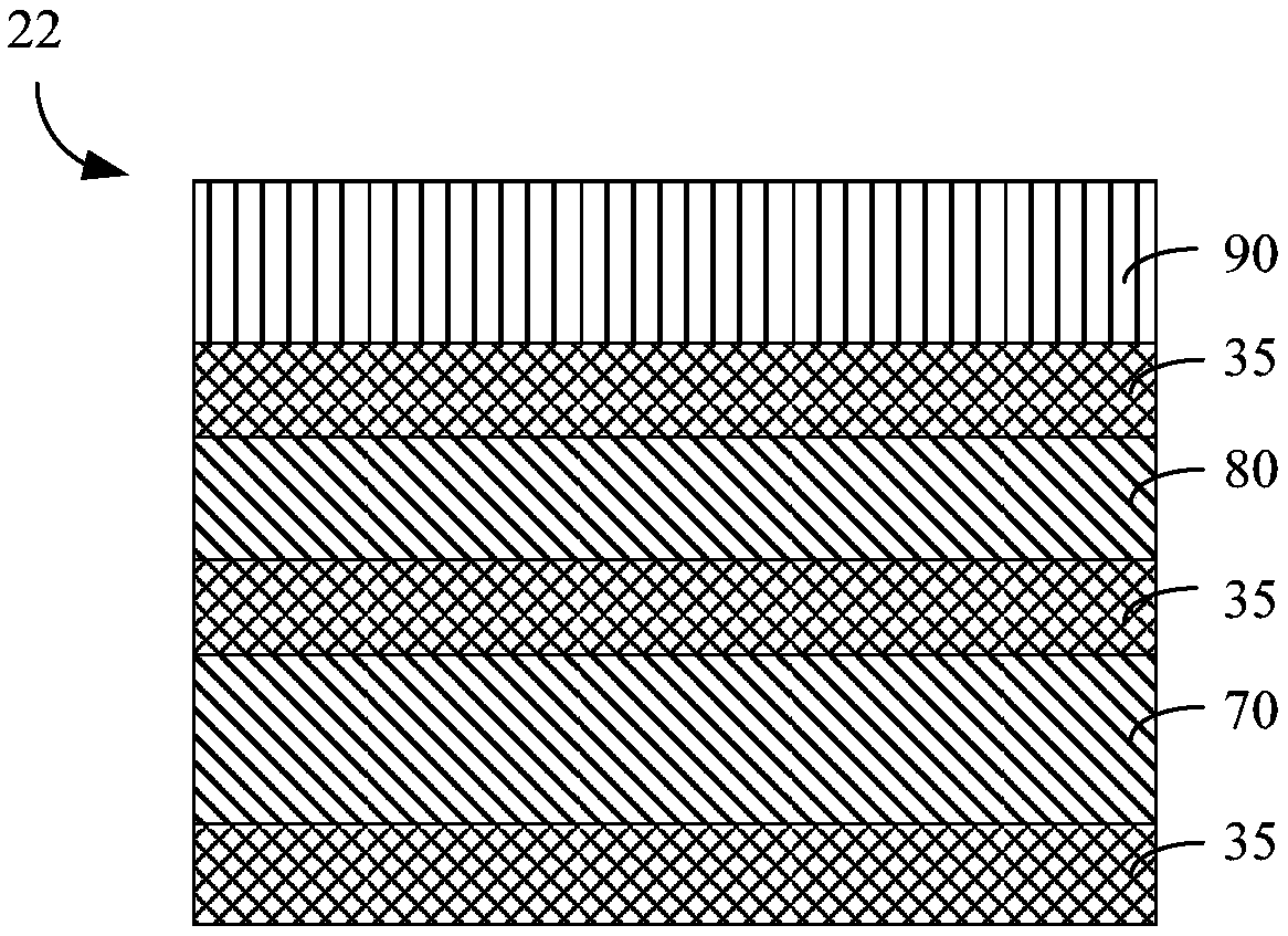
Moreover, the touch screen 22 with the added upper cover film layer 90 is relatively thick and costly, and it is difficult for consumers who pursue lightness, lightness and low cost to accept the introduction of high-cost and heavy touch screen 22 into the market.

Method used


Image

  • Liquid crystal touch screen and manufacturing method thereof
  • Liquid crystal touch screen and manufacturing method thereof
  • Liquid crystal touch screen and manufacturing method thereof

Examples


Embodiment 1

[0044] refer to Figure 4 , which is a schematic structural diagram of the liquid crystal touch screen 1 according to an embodiment of the present invention.

[0045] Such as Figure 4 As shown, one aspect of the present invention provides a liquid crystal touch screen 1 : it includes: a liquid crystal screen 100 and a touch screen 200 . The liquid crystal screen 100 includes: a first polarizer 110; a first glass substrate 120 disposed on the first polarizer 110; a liquid crystal layer 130 disposed on the glass substrate 120; a second glass A substrate 140 is disposed on the liquid crystal layer 130 ; and a color filter 150 is disposed on the second glass substrate 140 .

[0046] The touch screen 200 includes: a first conductive electrode layer 210; a second conductive electrode layer 220 disposed on the first conductive electrode layer 210; and a second polarizer 230 disposed on the first conductive electrode layer 220 on the second conductive electrode layer.

[0047] Ge...

Embodiment 2

[0053] refer to Figure 5 , which is a flowchart of a method for manufacturing a liquid crystal touch screen according to an embodiment of the present invention.

[0054] Such as Figure 5 As shown, one aspect of the present invention provides a method for manufacturing a liquid crystal touch screen, comprising the following steps:

[0055] Step S10: providing a first polarizer 110;

[0056] Step S20: setting a first glass substrate 120 on the first polarizer 110;

[0057] Step S30: setting a liquid crystal layer 130 on the glass substrate 120;

[0058] Step S40: setting a second glass substrate 140 on the liquid crystal layer 130;

[0059] Step S50: setting a color filter 150 on the second glass substrate 140;

[0060] Step S60: setting a first conductive electrode layer 210 on the color filter 150;

[0061] Step S70: disposing a second conductive electrode layer 220 on the first conductive electrode layer 210; and

[0062] Step S80: setting a second polarizer 230 on t...


PUM


Abstract

The invention provides a liquid crystal touch screen. The liquid crystal touch screen comprises a first polarizer, a first glass substrate arranged on the first polarizer, a liquid crystal layer arranged on the glass substrate, a second glass substrate arranged on the liquid crystal layer, a color light filter arranged on the second glass substrate, a first conductive electrode layer arranged on the color light filter, a second conductive electrode layer arranged on the first conductive electrode layer, and a second polarizer arranged on the second conductive electrode layer.

Description

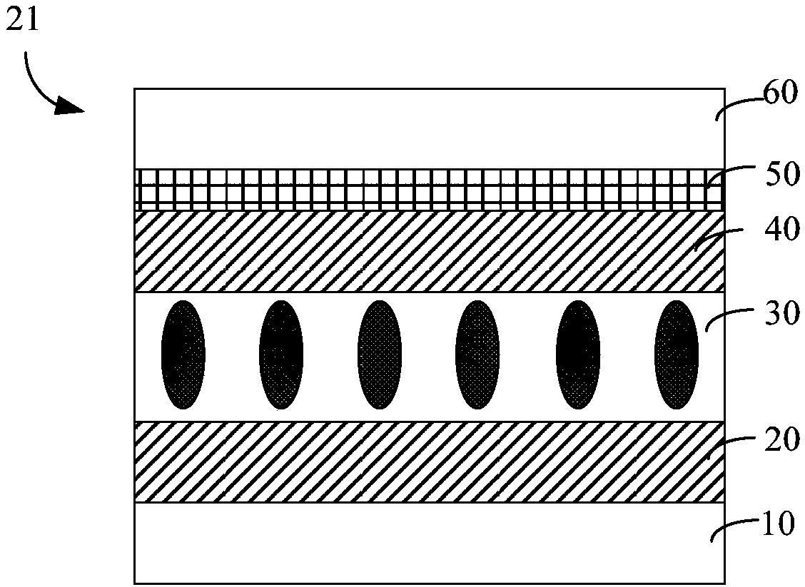
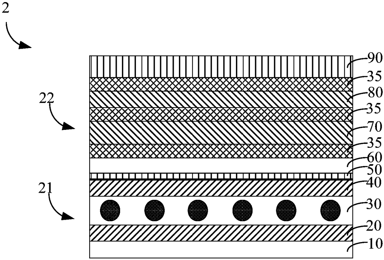
technical field [0001] The present invention relates to the field of display technology, and more specifically relates to a liquid crystal touch screen and a manufacturing method thereof, which are used to increase touch sensitivity, reduce cost, and reduce the weight and thickness of the liquid crystal touch screen. Background technique [0002] The liquid crystal capacitive touch screen 2 is composed of a liquid crystal display (LCD) 21 and a capacitive touch screen 22 . The liquid crystal screen 21 is composed of polarizers 10, 60, optical filters 50, glass substrates 20, 40 and a liquid crystal layer 30, and its schematic structural diagram is as follows figure 1 and image 3 As shown, the touch panel (TP) 22 has two layers of conductive plates 70 , 80 , and the conductive plates 70 , 80 are formed by etching different patterns on the film material by means of laser. The two layers of conductive electrode plates 70 and 80 are driving electrodes and receiving electrodes...

Claims


Application Information

Patent Timeline
Patent Type & Authority Applications(China)
IPC IPC(8): G02F1/1333G02F1/1335G06F3/044
CPCG02F1/1333G02F1/13338G02F1/133528G06F3/044
Inventor 陈蕾陈明暐康惠洋
Owner SHENZHEN CHINA STAR OPTOELECTRONICS SEMICON DISPLAY TECH CO LTD
Why Eureka
Try Eureka