Method of Improving Burr Condition on Flexible Substrate

A flexible substrate, burr technology, applied in nonlinear optics, instruments, optics, etc., can solve problems such as affecting ODF, high burr, and product yield decline

Active Publication Date: 2019-02-15
TRULY SEMICON
6 Cites 0 Cited by

AI-Extracted Technical Summary

Problems solved by technology

[0003] However, due to the limitations of the structure of the CF substrate during pre-cutting, a large number of high burrs will be formed...

Method used

Adopt dry etching to improve the cutting burr of above-mentioned flexible substrate, comprise the following steps:
Remove mask plate, coat developing solution tetramethylammonium hydroxide on photoresist surface, developing light-shielding area, exposes the part of corresponding light-shielding area in the surface of flexible substrate, carries out dry method to burr place area etch and eliminate burrs.
[0026] The present invention provides a method for improving the burr of the flexible substrate. After verification, it is found that after pre-cutting, one side of the flexible substrate will form a burr ...

Abstract

The invention relates to a method for improving burr condition on flexible substrates, which is used for reducing or eliminating burrs at the cutting edge after pre-cutting of flexible substrates, andadopting dry etching to reduce or eliminate the burrs. After verification, it is found that after pre-cutting, one side of a flexible substrate will form burrs at the cutting edge. The burrs can be treated by dry etching process to reduce the height of the burrs or even eliminate the burrs, so that the flexible substrate can meet the requirements of flat surface in the subsequent process, and toa large extent improve the yield of flexible substrates and the yield of the subsequent process, thus improves the production efficiency.

Application Domain

Non-linear optics

Technology Topic

EngineeringDry etching

Image

  • Method of Improving Burr Condition on Flexible Substrate
  • Method of Improving Burr Condition on Flexible Substrate

Examples

  • Experimental program(2)

Example Embodiment

[0037] Example 1
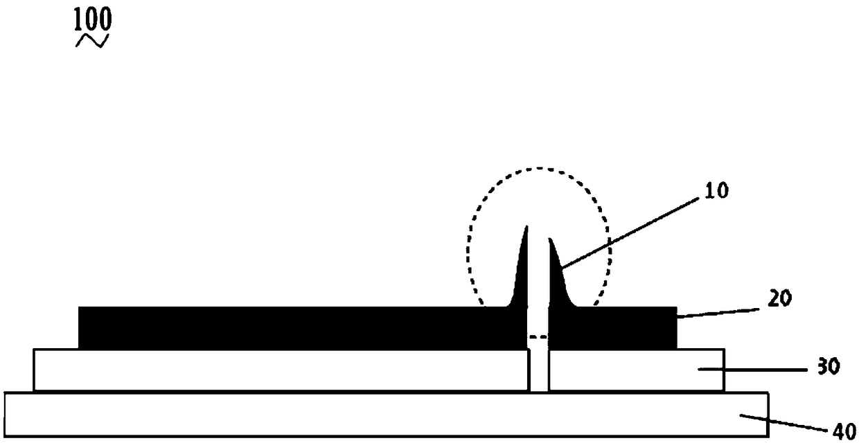
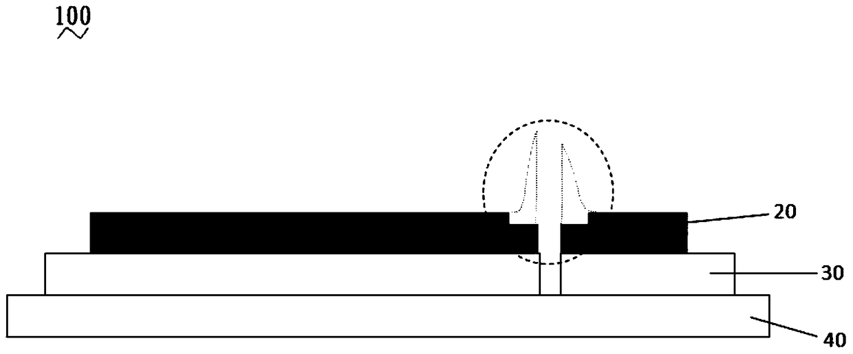
[0038] The flexible substrate in this embodiment is a CF substrate. After the flexible substrate is pre-cut and before the burrs are not improved, its structure is as follows figure 1 As shown, the flexible substrate includes a substrate, a flexible substrate and an insulating layer. The substrate and the insulating layer are respectively attached to both sides of the flexible substrate. The insulating layer is made of epoxy resin material, and the thickness of the insulating layer is 10 μm. The pre-cutting is to cut the flexible substrate and the insulation layer, and the cutting place forms a cutout, and after cutting, the insulation layer produces burrs at the cutout place.
[0039] Using dry etching to improve the cutting burr of the flexible substrate includes the following steps:
[0040] providing the above-mentioned flexible substrate;
[0041] Coat the burr side of the flexible substrate with photoresist to form a photoresist surface. The photoresist surface is provided with an exposure area and a light-shielding area, and the cut is located in the light-shielding area. , for exposure.
[0042] Remove the mask plate, apply developer tetramethylammonium hydroxide on the photoresist surface, develop the masked area, expose the part of the surface of the flexible substrate corresponding to the masked area, and perform dry etching on the area where the burr is located to eliminate glitch.
[0043] The conditions of dry etching are: the etching gas is O 2 , SF 6 , the sidewall shielding gas is CF 4 , the etching rate is 0.4 μm per minute, and the etching time is 30 minutes.
[0044] Flexible substrate after deburring such as figure 2 shown.

Example Embodiment

[0045] Example 2
[0046] The flexible substrate in this embodiment is a CF substrate. After the flexible substrate is pre-cut and before the burrs are not improved, the flexible substrate includes a base material, a flexible underlayment and an insulating layer. The base material and the insulating layer are respectively attached to both sides of the flexible underlayment. , the insulating layer is made of acrylic resin material, and the thickness of the insulating layer is 12 μm. The pre-cutting is to cut the flexible substrate and the insulation layer, and the cutting place forms a cutout, and after cutting, the insulation layer produces burrs at the cutout place.
[0047] Using dry etching to improve the cutting burr of the flexible substrate includes the following steps:
[0048] providing the above-mentioned flexible substrate;
[0049]Coat the burr side of the flexible substrate with photoresist to form a photoresist surface. The photoresist surface is provided with an exposure area and a light-shielding area, and the cut is located in the light-shielding area. , for exposure.
[0050] Remove the mask plate, apply developer tetramethylammonium hydroxide on the photoresist surface, develop the masked area, expose the part of the surface of the flexible substrate corresponding to the masked area, and perform dry etching on the area where the burr is located to eliminate glitch.
[0051] The conditions of dry etching are: the etching gas is O 2 , He, and the sidewall shielding gas is CF 4 , the etching rate is 0.5 μm per minute, and the etching time is 14 minutes.
[0052] The burrs of the flexible substrates in Examples 1 and 2 are all improved, and the burrs are reduced to the required height, and the flexible substrate is not damaged, which is conducive to the smooth progress of subsequent ODF and other processes.

PUM

PropertyMeasurementUnit
Thickness10.0µm
Thickness12.0µm

Description & Claims & Application Information

We can also present the details of the Description, Claims and Application information to help users get a comprehensive understanding of the technical details of the patent, such as background art, summary of invention, brief description of drawings, description of embodiments, and other original content. On the other hand, users can also determine the specific scope of protection of the technology through the list of claims; as well as understand the changes in the life cycle of the technology with the presentation of the patent timeline. Login to view more.
Why Eureka
Try Eureka