
A kind of output circuit and electronic device

A technology for output circuits and output stage circuits, applied in logic circuits, eliminating voltage/current interference, electrical components, etc., can solve problems such as logic errors, functional errors, and increased circuit area, so as to improve glitches and reduce impacts Effect

Active Publication Date: 2022-04-26
SEMICONDUCTOR MANUFACTURING INTERNATIONAL (BEIJING) CORP +1
View PDF7 Cites 0 Cited by
  • Summary
  • Abstract
  • Description
  • Claims
  • Application Information

AI Technical Summary

Problems solved by technology

For this reason, it is often necessary to use some resistors and capacitors to form a circuit that reduces burrs to control the burrs generated during signal transmission, otherwise some sensitive circuits will cause logic errors or functional errors due to the existence of burrs
However, adding or subtracting capacitance and resistance in the circuit to remove burrs will increase the circuit area, which is not conducive to circuit integration and will increase the cost

Method used


Image

  • A kind of output circuit and electronic device
  • A kind of output circuit and electronic device
  • A kind of output circuit and electronic device

Examples


Embodiment 1

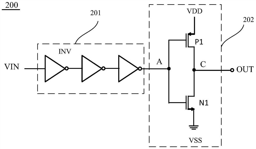
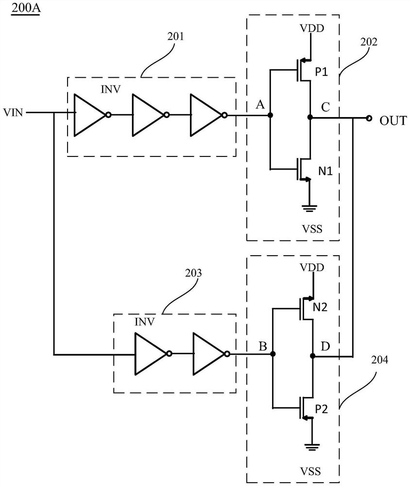
[0041] In order to better understand the present invention, the following combination Figure 2A and Figure 2B A schematic circuit according to an embodiment of the present invention is described in detail. in, Figure 2A shows a schematic circuit diagram of an existing output circuit; Figure 2B shows a schematic circuit diagram of an output circuit according to an embodiment of the invention, where Figure 2B The circuit shown is a pair of Figure 2A The circuit shown is improved.

[0042] Figure 2A As shown, the output circuit 200 includes a first input stage circuit 201 and a first output stage circuit 202 . The first input stage circuit 201 exemplarily includes three inverters INV connected in series. One end of the first input stage circuit 201 is connected to the input signal VIN of the output circuit 200, and the other end is connected to the first input of the first output stage circuit 202. Terminal A is connected. The first input stage circuit 201 generate...

Embodiment 2

[0054] Another embodiment of the present invention provides an electronic device, including the above-mentioned output circuit and an electronic component connected to the output circuit.

[0055] Wherein, the electronic component may be any electronic component such as a discrete device or an integrated circuit.

[0056] The electronic device of this embodiment can be any electronic product or equipment such as mobile phone, tablet computer, notebook computer, netbook, game console, TV set, VCD, DVD, navigator, camera, video recorder, voice recorder, MP3, MP4, PSP, etc. , can also be any intermediate product including the semiconductor device.

[0057] in, image 3 An example of a mobile phone is shown. The exterior of the mobile phone 300 is provided with a display portion 302 included in a case 301, operation buttons 303, an external connection port 304, a speaker 305, a microphone 606, and the like.

[0058] The electronic device in the embodiment of the present inventi...


PUM


Abstract

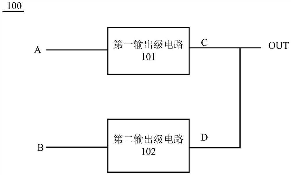
The invention provides an output circuit and an electronic device. The output circuit includes: a first output stage circuit, the first output stage circuit has a first input terminal and a first output terminal, the first input terminal is used to connect with the first input signal, and the first output terminal Connected to the output end of the output circuit, a first coupling capacitor is formed between the first input end and the first output end; a second output stage circuit, the second output stage circuit has a second input end and a second output terminal, the second input terminal is used to connect with the second input signal, the second output terminal is connected to the output terminal of the output circuit, the second input terminal and the second output terminal A second coupling capacitance is formed therebetween; wherein, the first coupling capacitance and the second coupling capacitance have opposite coupling effects. The output circuit can improve the burr at the output end and reduce the influence of the burr on the circuit. The electronic device has similar advantages.

Description

technical field [0001] The invention relates to the technical field of semiconductor integrated circuits, in particular to an output circuit and an electronic device. Background technique [0002] In integrated circuit applications, CMOS circuits occupy an important position. In the CMOS circuit, the delay is related to the length of the connection and the number of logic units, and is also affected by the manufacturing process, operating voltage, temperature and other conditions of the device, so the high and low level conversion of the signal also requires a certain transition time , so due to the existence of these two factors, when the level value of the multi-channel signal changes, the output of the combinational logic has a sequence at the moment of the signal change, and it does not change at the same time. In this process, some errors often occur spikes, these spikes are called "glitches". Generally, these burrs will be completely retained and passed to the next l...

Claims


Application Information

Patent Timeline
Patent Type & Authority Patents(China)
IPC IPC(8): H03K19/0948H03K19/003
CPCH03K19/00361H03K19/0948
Inventor 陈双文
Owner SEMICONDUCTOR MANUFACTURING INTERNATIONAL (BEIJING) CORP
Learn More