Array substrate and display panel thereof

An array substrate and substrate technology, applied in electrical components, electrical solid devices, circuits, etc., can solve problems such as large potential difference, affecting the quality of flat panel display panels or flat panel display devices, film breakdown, etc. Market competitiveness and the effect of improving product yield

Inactive Publication Date: 2019-02-15
HKC CORP LTD +1
View PDF5 Cites 1 Cited by
  • Summary
  • Abstract
  • Description
  • Claims
  • Application Information

AI Technical Summary

Problems solved by technology

Generally speaking, during the process of coating and substrate handling, the contact between the substrate and other media will generate a large amount of static charge, which accumulates on the array substrate, and will form a large potential difference when it contacts with the transmission equipment. Further, the film layer near the contact point will be broken down, seriously affecting the quality of the flat panel display panel or flat panel display device

Method used


Image

  • Array substrate and display panel thereof
  • Array substrate and display panel thereof
  • Array substrate and display panel thereof

Examples


Embodiment Construction

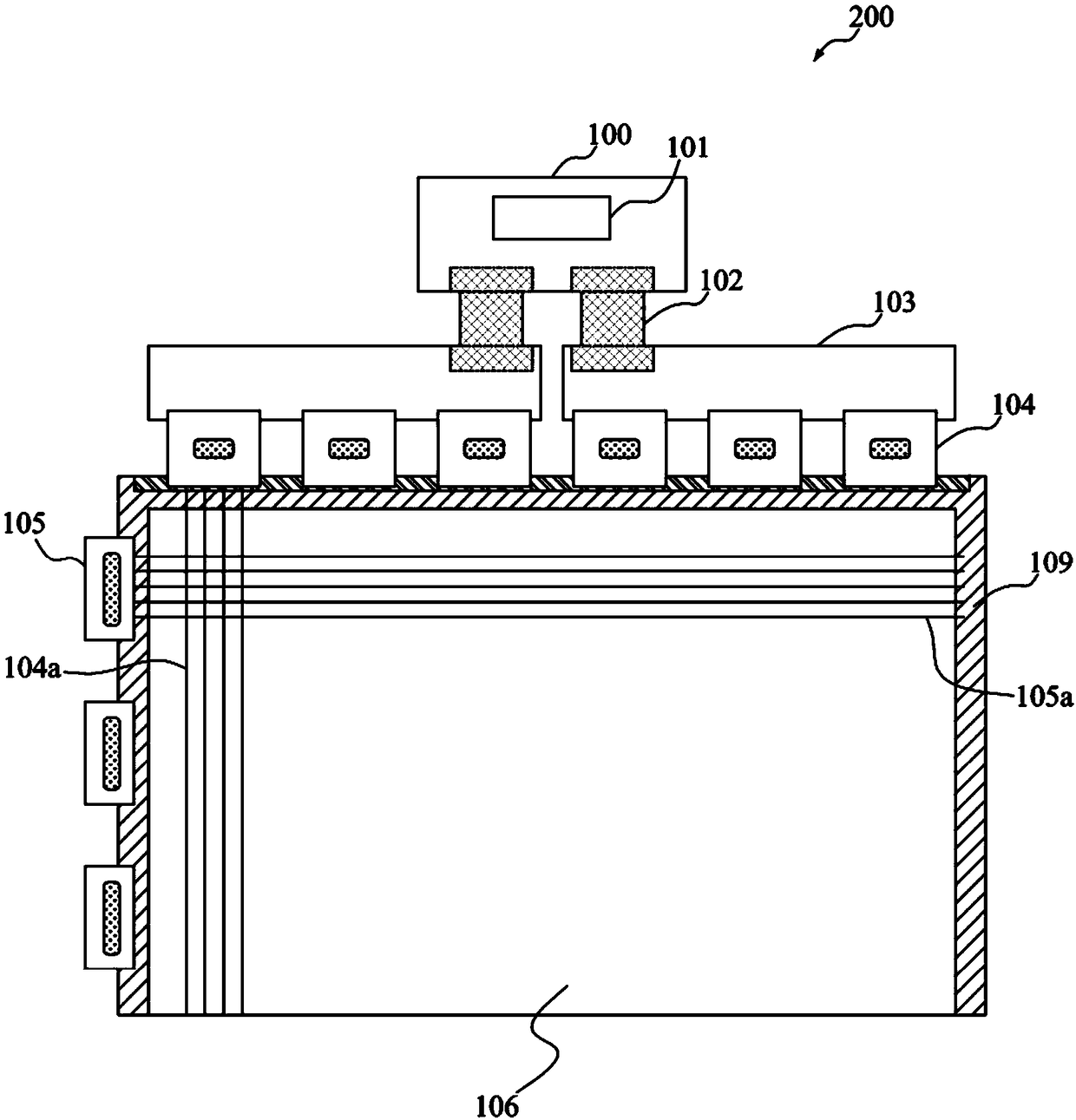
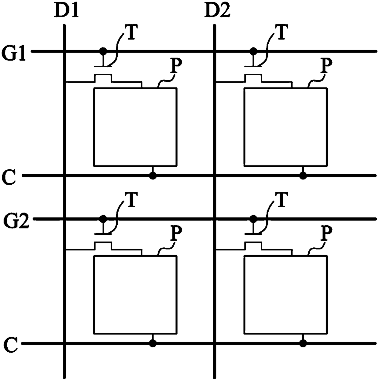
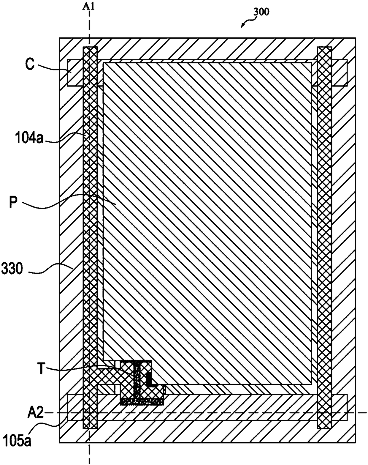
[0036]The following descriptions of the various embodiments refer to the attached drawings to illustrate specific embodiments that the present application can be implemented in. The directional terms mentioned in this application, such as "up", "down", "front", "rear", "left", "right", "inside", "outside", "side", etc., are for reference only The orientation of the attached schema. Therefore, the directional terms used are used to illustrate and understand the application, but not to limit the application.

[0037] The drawings and descriptions are to be regarded as illustrative in nature and not restrictive. In the figures, structurally similar units are denoted by the same reference numerals. In addition, the size and thickness of each component shown in the drawings are arbitrarily shown for understanding and convenience of description, but the present application is not limited thereto.

[0038] In the drawings, the thickness of layers, films, panels, regions, etc., are...


PUM


Abstract

The invention provides an array substrate and a display panel thereof. The array substrate comprises a substrate and a plurality of driving wire sections, wherein the substrate comprises a display area, and the display are is configured with a plurality of driving switches and a plurality of pixel electrodes; the plurality of pixel electrodes are electrically coupled to the plurality of driving switches; the plurality of driving wire segments are arranged on the substrate and are electrically coupled to the plurality of driving switches; each driving wire segment comprises an insulating layer,a protection layer and a metal layer, wherein the insulating layer is arranged on the substrate; the protection layer is arranged on the substrate; the protection layer covers the insulating layer; the metal layer is arranged in the coverage range of the driving wire segment, and the metal layer is in floating connection, wherein the metal layer is arranged between the substrate and the insulating layer, and on at least one part between the insulation layer and the protection layer. By means of the floating connection metal layer, the electrostatic discharge path is increased, and even if thefloating connection metal layer is burnt out, the display quality cannot be influenced, and the product yield can be relatively improved. Meanwhile, only the mask graph needs to be adjusted, so thatthe production process does not need to be adjusted.

Description

technical field [0001] The present application relates to the display field, in particular to an array substrate and a display panel thereof. Background technique [0002] The flat panel display device has many advantages such as wide color gamut and power saving, and is widely used in various fields. Existing flat panel display devices mainly include liquid crystal display (Liquid Crystal Display, LCD), organic light emitting diode (Organic Light Emitting Diodes, OLED) display device and quantum dot light emitting diode (Quantum DotLight Emitting Diodes, QLED) display device. Among them, a thin film transistor (Thin Film Transistor, TFT), which can be formed on a glass substrate or a plastic substrate, is usually used as an active switch and is one of the important components of a flat panel display device. With the development, more and higher requirements are put forward for display panels and display devices, such as antistatic performance. Due to the high sensitivity o...

Claims


Application Information

Patent Timeline
Patent Type & Authority Applications(China)
IPC IPC(8): H01L27/12H01L27/32
CPCH01L27/1214H01L27/124H01L27/1259H10K59/123H10K59/131
Inventor 吴川
Owner HKC CORP LTD
Why Eureka
Try Eureka