Level shifting circuit

A level shift circuit and level shift technology, applied in the direction of logic circuit, logic circuit interface device, logic circuit connection/interface layout, etc., can solve the problems of high power consumption, low level speed and speed, and reduce the signal Changeover times, improved manufacturability, size-insensitive effects

Inactive Publication Date: 2019-02-15
SHANGHAI EASTSOFT MICROELECTRONICS
View PDF8 Cites 5 Cited by
  • Summary
  • Abstract
  • Description
  • Claims
  • Application Information

AI Technical Summary

Problems solved by technology

[0004] However, existing level-shifting circuits have low speed for level-to-level rotation and high power consumption

Method used


Image

  • Level shifting circuit
  • Level shifting circuit
  • Level shifting circuit

Examples


Embodiment Construction

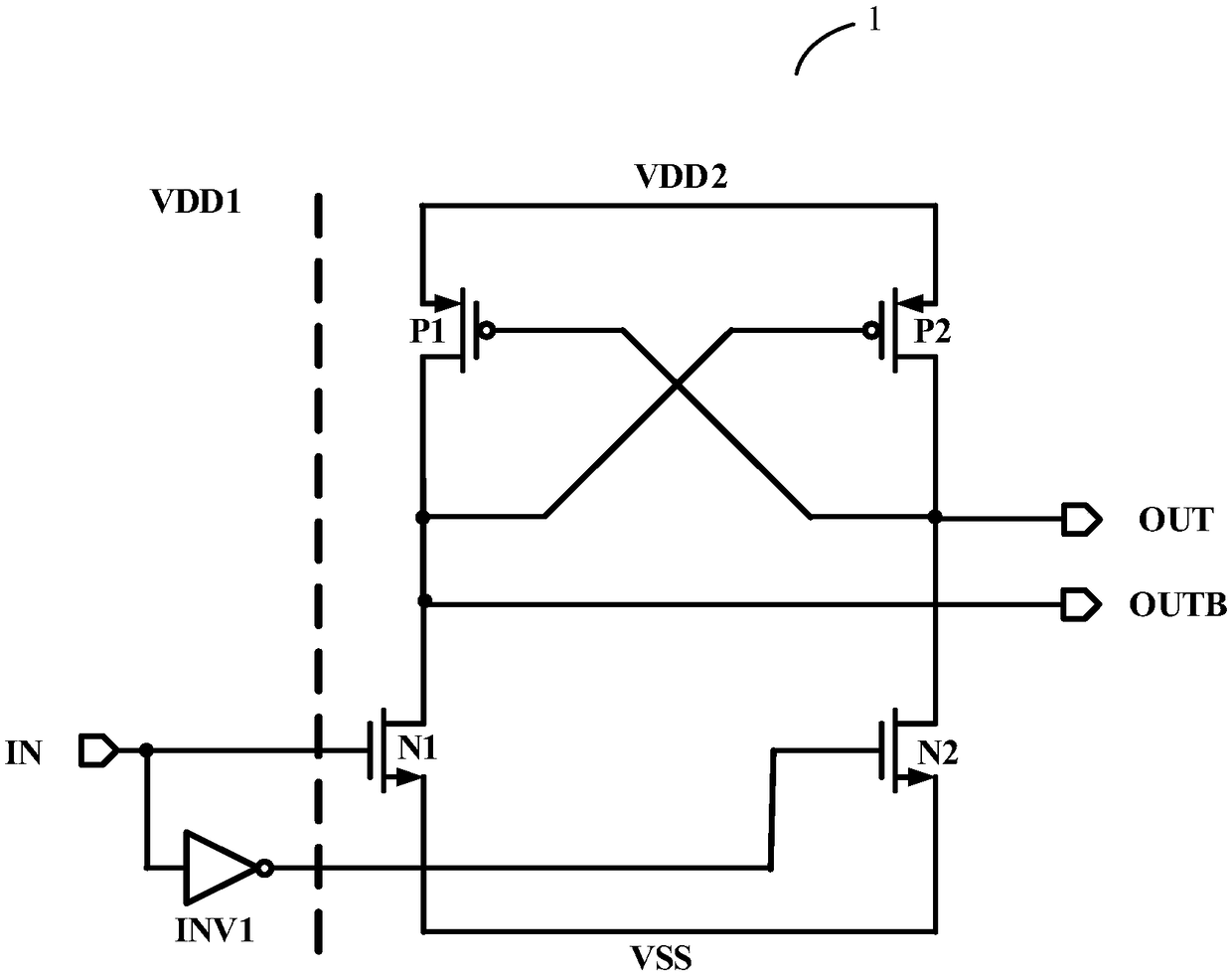
[0029] figure 1 It is a structural schematic diagram of a level shift circuit 1 in the prior art. refer to figure 1 , The level shift circuit 1 includes: a first PMOS transistor P1, a second PMOS transistor P2, a first NMOS transistor N1, a second NMOS transistor N2, and an inverter INV1.

[0030] The inverter INV1 and the signal IN output from the low-voltage signal output terminal (that is, the input signal of the level shift circuit, hereinafter referred to as the input signal) all work in the low-voltage domain VDD1, and the first PMOS transistor P1, the second PMOS transistor P2, and the second PMOS transistor P2 Both the first NMOS transistor N1 and the second NMOS transistor N2 work in the high voltage domain VDD2, and the output signal OUT of the first output terminal and the output signal OUTB of the second output terminal are opposite in logic, and also work in the high voltage domain VDD2.

[0031] In a steady state, when the input signal IN is at a low level (ie ...


PUM


Abstract

The invention discloses a level shifting circuit comprising a phase inverter and a level shifting unit; the level shifting unit comprises a first NMOS transistor, a second NMOS transistor, a first PMOS transistor, a second PMOS transistor and a confrontation isolating circuit; the grid of the NMOS transistor is coupled with a low-voltage signal output end; the low-voltage signal output end is coupled with the grid of the second NMOS transistor via the phase inverter; the drain of the first NMOS transistor serves as a first output end; the drain of the second NMOS transistor serves as a secondoutput end; the confrontation isolating circuit is coupled between the PMOS transistors and the NMOS transistors of the level shifting circuit, and applicable to isolating confrontation between the coupled PMOS transistors and NMOS transistors during the process that the level shifting circuit performs level shifting. With the application of the scheme of the circuit, the time of confrontation between the PMOS transistors and the NMOS transistors during the level shifting process can be effectively shortened, and the penetrating current generated during the level shifting process can be reduced; therefore, the level shifting speed is improved and the power consumption is reduced, the application requirements on high speed, low voltage and low power consumption are met.

Description

technical field [0001] The invention relates to the field of semiconductor integrated circuits, in particular to a level shift circuit. Background technique [0002] Driven by the development of the Internet of Things, handheld devices emerge in an endless stream, which makes the integration of chips continue to increase, and the integration of functional modules in different voltage domains is becoming more and more common. As an interface circuit for communication between different voltage domains, level shifting circuits are crucial. [0003] The level shift circuit is mainly used to convert the high-level signal and low-level signal in the low-voltage domain into the corresponding high-level signal and low-level signal in the high-voltage domain. In practical applications, due to the further reduction of the power supply voltage of the corresponding voltage domain inside the chip, the reliable operation of the level shift circuit at a lower voltage is a challenge, and t...

Claims


Application Information

Patent Timeline
Patent Type & Authority Applications(China)
IPC IPC(8): H03K19/0175H03K19/00H03K19/01
CPCH03K19/0008H03K19/01H03K19/017509
Inventor 卢月娟袁俊陈光胜
Owner SHANGHAI EASTSOFT MICROELECTRONICS
Why Eureka
Try Eureka