Supercharge Your Innovation With Domain-Expert AI Agents!

Flattening and fastening device for 12-inch wafers

A fixing device and flattening technology, applied in semiconductor/solid-state device manufacturing, electrical components, circuits, etc., can solve problems such as affecting subsequent processes, unable to flatten and fix, and achieve the effect of avoiding omission and good flatness

Active Publication Date: 2019-02-19
SHANGHAI WEISONG IND AUTOMATION +1
View PDF4 Cites 0 Cited by
  • Summary
  • Abstract
  • Description
  • Claims
  • Application Information

AI Technical Summary

Problems solved by technology

[0004] The present invention is to solve the above-mentioned problem that the warpage of the wafer cannot be flattened and fixed to affect the subsequent process, and the purpose is to propose a flattening and fixing device for a 12-inch wafer

Method used


Image

  • Flattening and fastening device for 12-inch wafers
  • Flattening and fastening device for 12-inch wafers
  • Flattening and fastening device for 12-inch wafers

Examples


Embodiment Construction

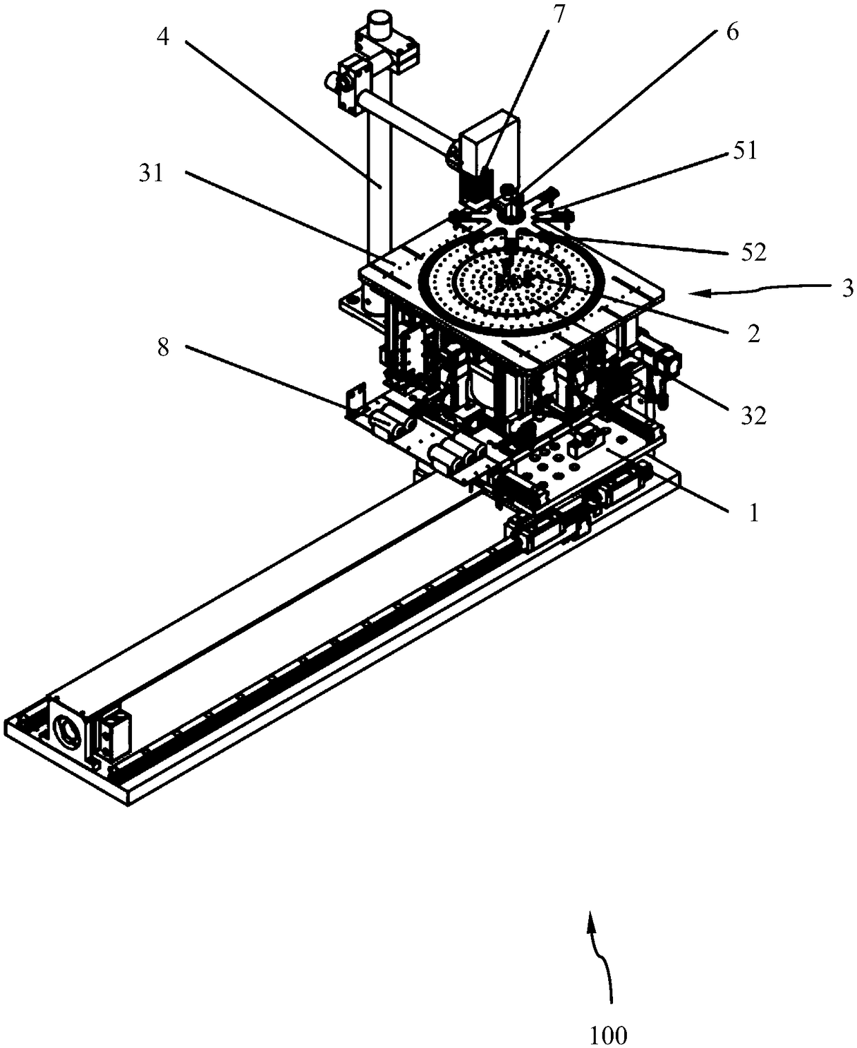
[0025] In order to make the technical means realized by the present invention, creative features, goals and effects easy to understand, the following embodiments are combined with the accompanying drawings to explain the composition, working principle, implementation method and beneficial effects of the 12-inch wafer flattening device provided by the present invention. Be specific.

[0026] figure 1 It is a structural schematic diagram of a flattening and fixing device for a 12-inch wafer in an embodiment of the present invention.

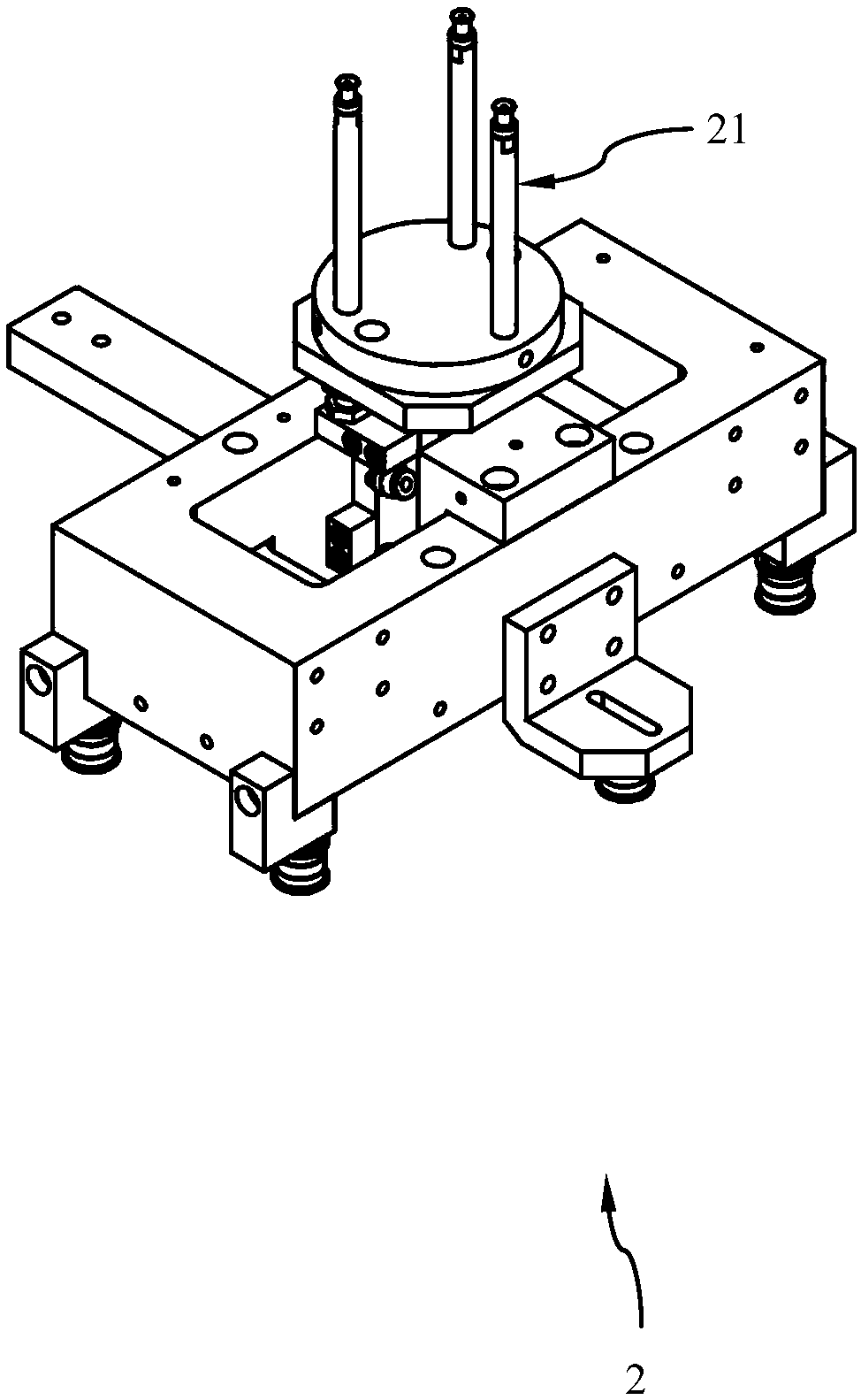
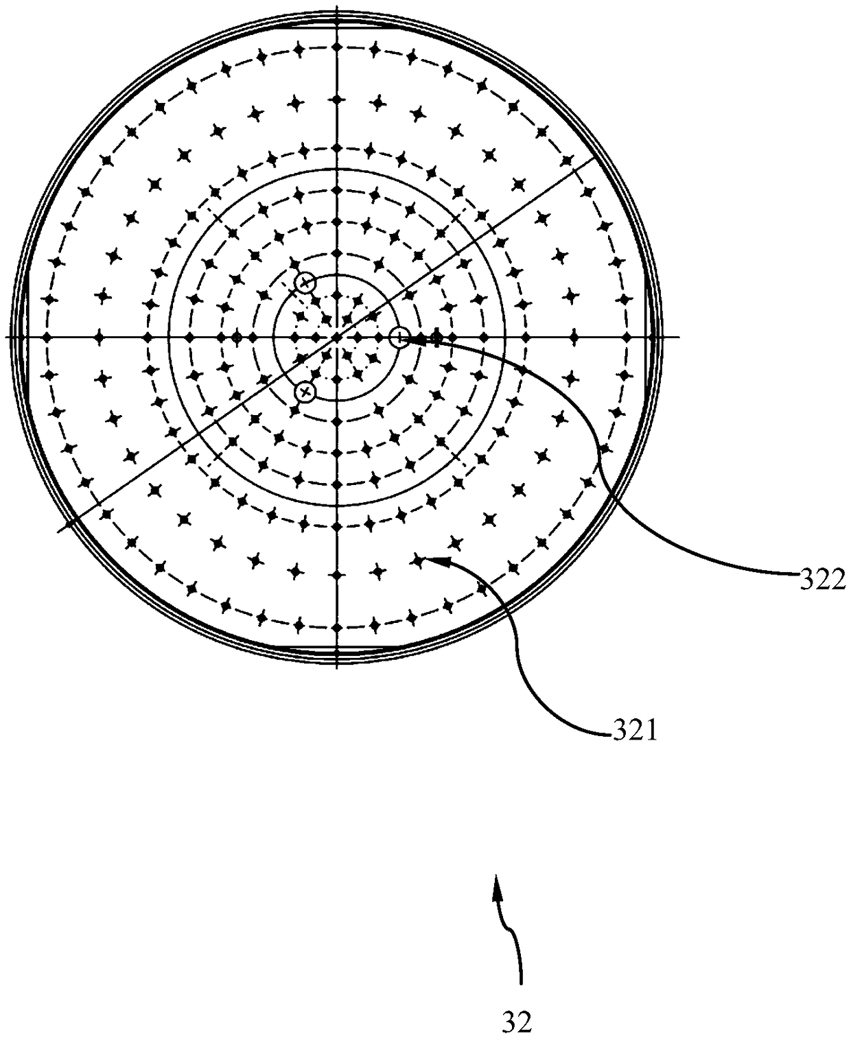
[0027] Such as figure 1 As shown, the 12-inch wafer flattening and fixing device 100 in this embodiment is used to flatten and fix warped wafers placed in packaging equipment, and has a carrier table 1, an adsorption fixing part, a crimping fixing part, a detection part and control department.

[0028] The carrying platform 1 is installed in the packaging equipment and can move horizontally between various stations in the packaging equipment.

...


PUM

PropertyMeasurementUnit
Diameteraaaaaaaaaa

Abstract

A flattening and fastening device for 12-inch wafers comprises a carrying platform, an attracting and fastening portion mounted on the carrying platform, and a detecting portion for detecting the flatness of warped wafers. The detecting portion comprises a negative pressure detecting unit and a flatness detecting unit. The attracting and fastening portion comprises a pre-fastening unit, a loadingand fastening unit, and a negative pressure unit for respectively providing vacuum negative pressure to the pre-fastening unit and the loading and fastening unit; the pre-fastening unit is mounted onthe carrying platform, can move up and down relative to the carrying platform, and is used for pre-fastening the warped wafers; the loading and fastening unit is mounted on the carrying platform, canmove up and down relative to the carrying platform, is used for loading and fastening the warped wafers, and is provided with a base plate, a plurality of attraction holes and a plurality of base plate through holes, the attraction holes and the base plate through holes are formed in the base plate, and the base plate through holes are located in the central area of the base plate to allow the pre-fastening unit to pass. When the warped wafers are pre-fastened by the pre-fastening unit, the loading and fastening unit starts the negative pressure to attract and fasten the pre-fastened warped wafers.

Description

technical field [0001] The invention relates to a fixing device. Background technique [0002] Fan Out WLP (Fan-Out Wafer Level Packaging; FOWLP) is a high-end packaging technology that uses solder balls instead of traditional DIP pins to achieve higher integration in a single-chip package , has better electrical properties, and can reduce packaging costs, increase computing speed, and reduce power consumption. However, in some process steps of fan-out wafer level packaging, such as die deposition, die bonding, etc., due to the uneven pressure, the flatness of the silicon wafer and the pressure on the die are affected, resulting in wafer warping warp, and the reconstructed wafer contains plastic, silicon and metal materials, and the ratio of silicon to colloid is different in the X, Y, and Z directions. The thermal expansion and contraction of the mold during heating and cooling will cause the wafer to warp . [0003] Wafer surface unevenness caused by wafer warpage is a ...

Claims


Application Information

Patent Timeline
IPC IPC(8): H01L21/683H01L21/67H01L21/68H01L21/687
CPCH01L21/67092H01L21/67288H01L21/68H01L21/6838H01L21/68721
Inventor 刘劲松郭俭张金志崔恒彬邵志翔
Owner SHANGHAI WEISONG IND AUTOMATION
Features
  • R&D
  • Intellectual Property
  • Life Sciences
  • Materials
  • Tech Scout
  • Unparalleled Data Quality
  • Higher Quality Content
  • 60% Fewer Hallucinations
Learn More