Pixel Array Substrate

A technology of pixel array substrate and pixel structure, applied in semiconductor/solid-state device parts, capacitors, semiconductor devices, etc., can solve problems such as abnormal display, collapse, short circuit, etc., achieve improvement of short circuit problem, increase storage capacitance, and process margin Enhanced effect

Active Publication Date: 2020-09-25
AU OPTRONICS CORP
View PDF4 Cites 0 Cited by
  • Summary
  • Abstract
  • Description
  • Claims
  • Application Information

AI Technical Summary

Problems solved by technology

However, when patterning the second insulating material layer to form the second contact window, part of the top surface and sidewalls of the first insulating layer are easily removed during the formation process of the second contact window and collapse occurs, resulting in The uppermost auxiliary electrode is in contact with the pixel electrode and is short-circuited, resulting in abnormal display

Method used


Image

  • Pixel Array Substrate
  • Pixel Array Substrate
  • Pixel Array Substrate

Examples


Embodiment Construction

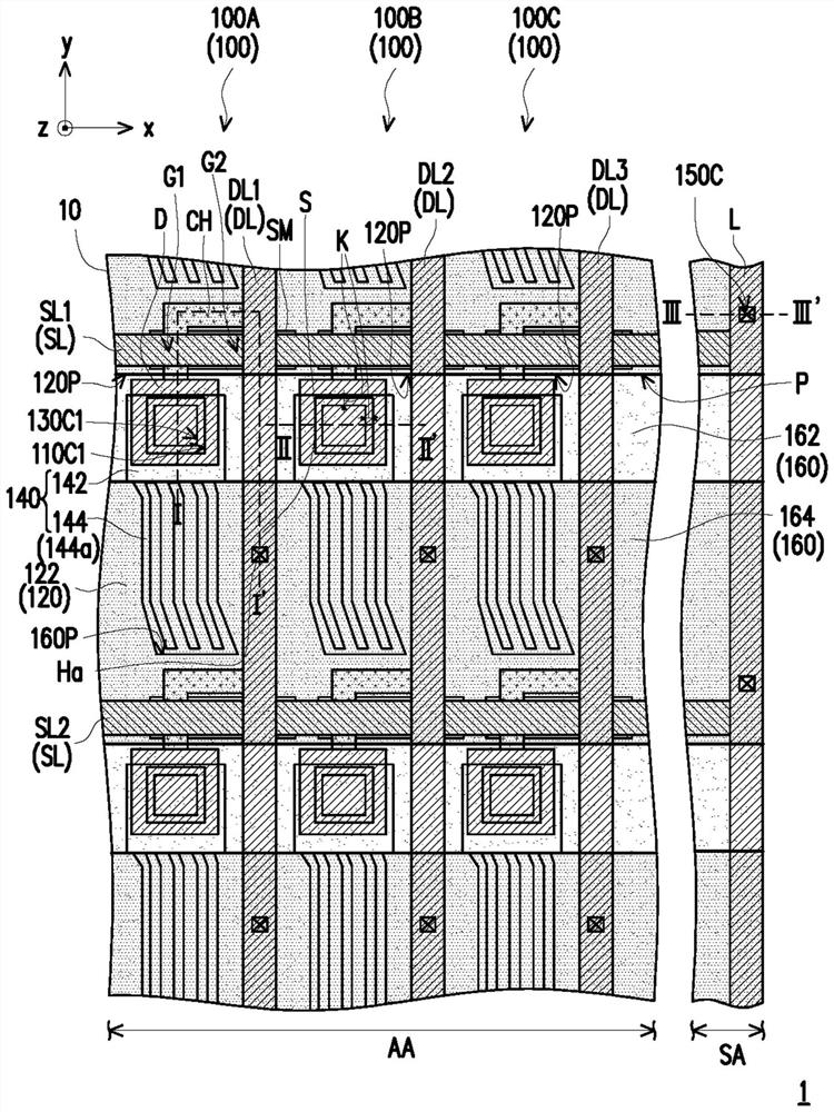
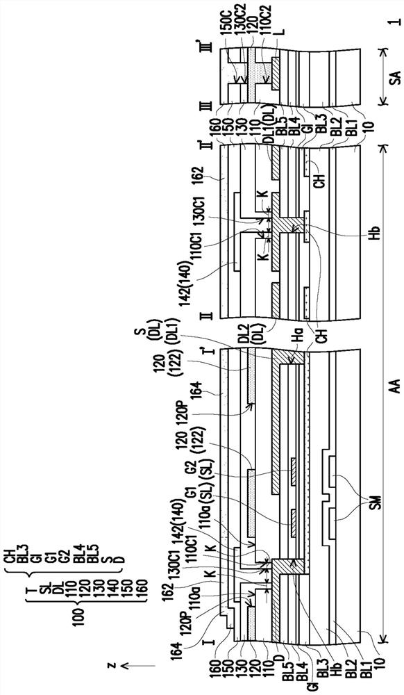
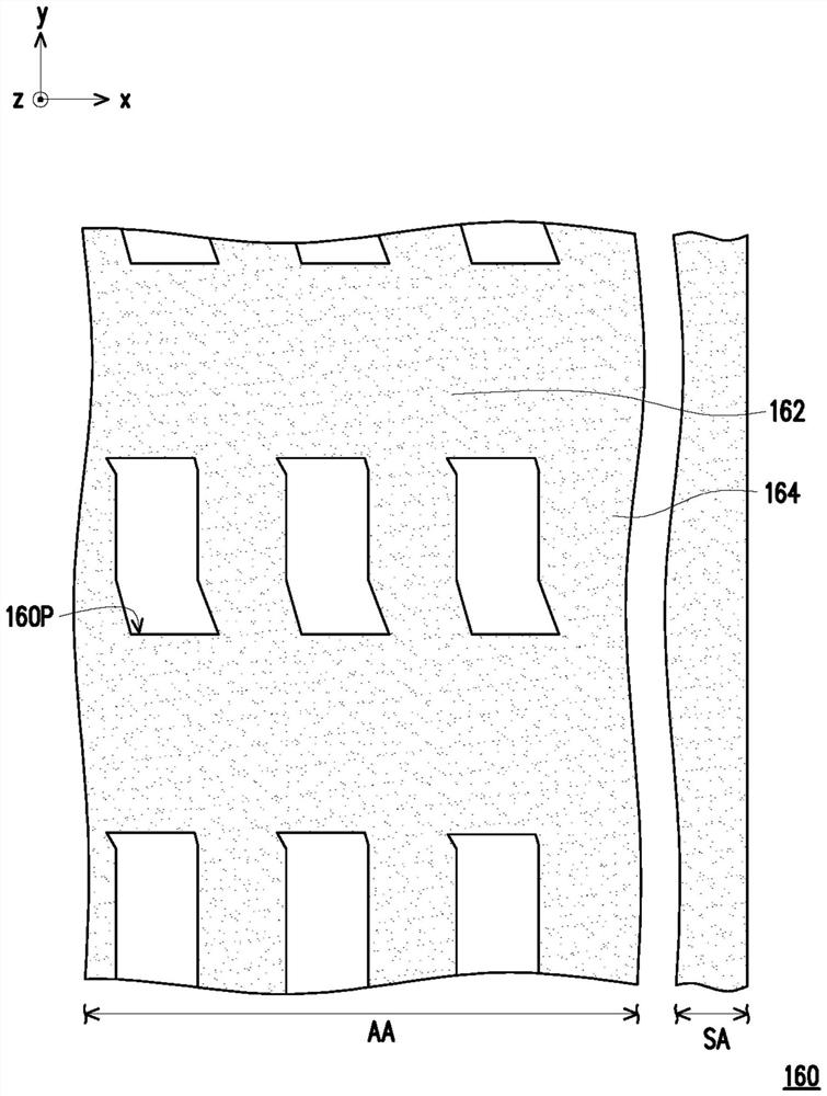
[0072] figure 1 It is a schematic top view of a pixel array substrate 1 according to an embodiment of the present invention. figure 2 based on figure 1 The schematic cross-sectional view of the pixel array substrate 1 drawn by the section lines I-I', II-II' and III-III'. image 3 Shown is figure 1 A schematic top view of the film layer to which the auxiliary electrode 160 of the pixel array substrate 1 belongs.

[0073] Please refer to figure 1 and figure 2 , the pixel array substrate 1 includes a substrate 10 and a plurality of pixel structures 100 . The substrate 10 has an active area AA and a peripheral area SA outside the active area AA. A plurality of pixel structures 100 are disposed on the active area AA of the substrate 10 . Each pixel structure 100 includes scan lines SL, data lines DL and thin film transistors T arranged alternately with the scan lines SL. In this embodiment, the scan lines SL1 and SL2 extend in the direction x, and the first data line DL1 ...


PUM


Abstract

A pixel array substrate includes a substrate and a plurality of pixel structures. The substrate has an active area. A plurality of pixel electrodes are disposed on an active region of the substrate. Each of the pixel structures includes a scan line, a data line, a thin film transistor, a first insulating layer, a common electrode, a second insulating layer, a pixel electrode, a third insulating layer, and an auxiliary electrode. A second contact window of the second insulating layer overlaps a first contact window of the first insulating layer and is located within a first opening of the common electrode. The pixel electrode is disposed on the second insulating layer and electrically connected to the second end of the thin film transistor through the first contact window. The auxiliary electrode is disposed on the third insulating layer and electrically connected to the common electrode. The auxiliary electrode has a second opening that overlaps the pixel electrode, and a first solid portion of the auxiliary electrode shields the first opening.

Description

technical field [0001] The present invention relates to a substrate, and in particular to a pixel array substrate. Background technique [0002] In recent years, people's demand for high-resolution display panels has gradually increased. However, when the resolution of the display panel increases, it means that the size of the pixels in the display panel must be reduced, thus testing whether the process capability complies with stricter design rules. In order to reduce the load on the process machine and increase the feasibility of the process, designing an appropriate pixel layout has become an important issue. [0003] In the high-resolution pixel structure, the size of each pixel becomes smaller, so the storage capacitance of each pixel structure also becomes smaller, resulting in a lower ability to maintain the brightness of the pixel. At present, in order to increase the size of the storage capacitor, the common electrode and the auxiliary electrode are generally arra...

Claims


Application Information

Patent Timeline
Patent Type & Authority Patents(China)
IPC IPC(8): H01L27/12H01L23/64
CPCH01L27/124H01L27/1255H01L28/40
Inventor 苏志中陈亦伟
Owner AU OPTRONICS CORP
Why Eureka
Try Eureka