Epitaxial material for N-face light emergence AlGaInP LED thin film chips and preparation method of epitaxial material

A technology of thin-film chips and epitaxial materials, applied in the direction of electrical components, circuits, semiconductor devices, etc., can solve the problems of low electro-optical conversion efficiency, achieve the effects of eliminating light absorption, improving adhesion, and simplifying the preparation process

Active Publication Date: 2019-02-19
NANCHANG UNIV +1
View PDF5 Cites 5 Cited by
  • Summary
  • Abstract
  • Description
  • Claims
  • Application Information

AI Technical Summary

Problems solved by technology

However, the epitaxial material grown directly on the GaAs substrate has two major disadvantages of substrate absorption and total reflection loss by preparing N electrodes on the substrate side and P electrodes on the upper surface, and the electro-optical conversion efficiency is very low, generally less than 10. %

Method used


Image

  • Epitaxial material for N-face light emergence AlGaInP LED thin film chips and preparation method of epitaxial material
  • Epitaxial material for N-face light emergence AlGaInP LED thin film chips and preparation method of epitaxial material

Examples


Embodiment Construction

[0026] Below in conjunction with accompanying drawing, the present invention will be further described.

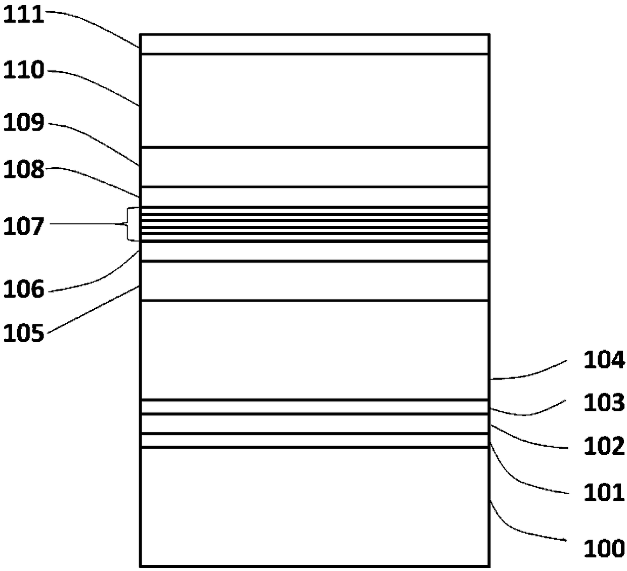
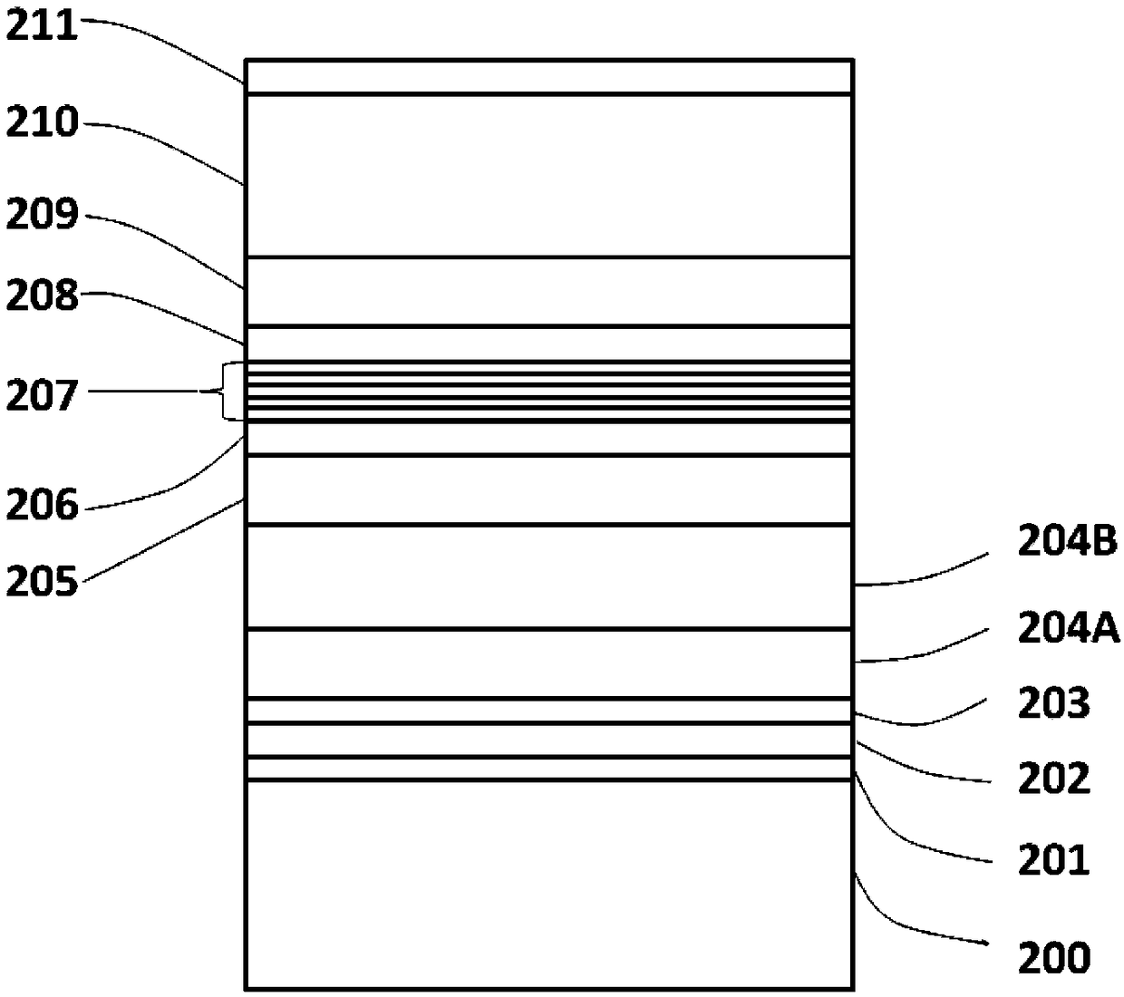
[0027] figure 2It is a schematic structural diagram of an epitaxial material for an N-surface light-emitting AlGaInP LED thin film chip of the present invention. According to the sequence of epitaxial growth, it includes an N-type GaAs substrate 200, an N-type GaAs buffer layer 201, and a first etch layer from bottom to top. Barrier layer 202, second corrosion barrier layer 203, first N-type roughened layer 204A, second N-type roughened layer 204B, N-type confinement layer 205, N-side space layer 206, multiple quantum well light-emitting region 207, P-side The space layer 208 , the P-type confinement layer 209 , the P-type current spreading layer 210 and the P-type ohmic contact layer 211 .

[0028] The (Al x1 Ga 1-x1 ) y1 In 1-y1 1P material with a forbidden band width than that used in the quantum wells of the multi-quantum well light-emitting region 207 (Al x5 Ga...


PUM


Abstract

The invention discloses an epitaxial material for N-face light emergence AlGaInP LED thin film chips and a preparation method of the epitaxial material. The epitaxial material comprises an N-type GaAssubstrate, an N-type GaAs buffer layer, a first corrosive barrier layer, a second corrosive barrier layer, a first N-type roughened layer, a second N-type roughened layer, an N-type limiting layer, an N-side space layer, a multiple quantum well illuminant area, a P-side space layer, a P-type limiting layer, a P-type current expanding layer and a P-type ohmic contact layer. The invention further discloses a preparation method of the epitaxial material for the N-face light emergence AlGaInP LED thin film chips. An N electrode can be directly prepared on the first N-type roughened layer, the problem of light absorption of the ohmic contact layer is eliminated, adhesion of the N electrode can be improved, a preparation process of the N-face light emergence AlGaInP LED thin film chips is simplified, and the chip index is effectively increased while cost reduction is realized.

Description

technical field [0001] The invention belongs to the field of semiconductor light-emitting devices, and in particular relates to an epitaxial material for AlGaInP LED thin-film chips used for emitting light from an N surface and a preparation method thereof. Background technique [0002] Semiconductor light-emitting diodes (Light-Emitting Diodes, LEDs) have been widely used in many fields, and are recognized as a next-generation green lighting source. The AlGaInP material lattice-matched with the GaAs substrate can cover visible light wavelengths from 560nm to 650nm, and is an excellent material for preparing red to yellow-green LEDs. AlGaInP light-emitting diodes have important applications in the field of solid-state lighting and display, such as full-color screen displays, automotive lights, backlights, traffic lights, and daily lighting. [0003] In recent years, people have made great progress in the growth technology of AlGaInP light-emitting diode epitaxial materials,...

Claims


Application Information

Patent Timeline
Patent Type & Authority Applications(China)
IPC IPC(8): H01L33/22H01L33/30H01L33/00
CPCH01L33/0062H01L33/22H01L33/30Y02P70/50
Inventor 李树强江风益刘军林王光绪陈芳郭醒
Owner NANCHANG UNIV
Why Eureka
Try Eureka