Display panel and method for manufacturing same

A technology for display panels and manufacturing methods, applied in semiconductor/solid-state device manufacturing, electrical components, electric solid-state devices, etc., can solve problems such as abnormal display, failure of cathode, connection of auxiliary electrodes, etc., achieve uniform display and improve voltage drop problems Effect

CN109360900AActive Publication Date: 2019-02-19SHENZHEN CHINA STAR OPTOELECTRONICS SEMICON DISPLAY TECH CO LTD
6 Cites 26 Cited by

Patent Information

Authority / Receiving Office
CN · China
Patent Type
Applications(China)
Current Assignee / Owner
Publication Date
2019-02-19

Smart Images

  • Figure 1
    Figure 1
  • Figure 2
    Figure 2
  • Figure 3
    Figure 3
Patent Text Reader

Abstract

The invention discloses a display panel and a method for manufacturing the same. The display panel is characterized in that an auxiliary electrode and a positive electrode of the display panel are arranged on a substrate, a pixel definition layer covers the auxiliary electrode and the positive electrode, the positive electrode and the auxiliary electrode are partially exposed, a negative electrodeisolation column is arranged on exposed portions of the auxiliary electrode, an isolation table of the negative electrode isolation column is electrically conductive and is in contact with the auxiliary electrode, an isolation column body of the negative electrode isolation column is arranged in the isolation table, and a luminescent layer covers the pixel definition layer and exposed portions ofthe positive electrode and the auxiliary electrode and is partitioned by the negative electrode isolation column; a negative electrode covers the luminescent layer, is partitioned by the negative electrode isolation column and is at least in contact with the isolation table. Owing to the mode, the display panel and the method have the advantages that the negative electrode and the auxiliary electrode can be effectively electrically connected with each other, the negative electrode can be individually controlled, and accordingly uniform display effects can be realized by the display panel.
Need to check novelty before this filing date? Find Prior Art

Description

technical field

[0001] The present application relates to the field of display technology, in particular to a display panel and a manufacturing method thereof. Background technique

[0002] Because Organic Light-Emitting Diode (OLED) has display characteristics and quality beyond Liquid Crystal Display (LCD), such as thinner and lighter, short response time, low driving voltage, better display color and Display viewing angle and other advantages, it has received widespread attention. In recent years, the development of OLED has been changing with each passing day. Not only can it produce curved displays, but it is also gradually developing to large sizes. However, there is a problem of voltage drop in the large size, especially for the top emission display panel, the problem of voltage drop caused by the thin cathode needs to be solved urgently, so the auxiliary electrode and cathode isolation column are made in the process to separate the cathode to achieve separate contro...

Examples

Embodiment Construction

[0013] The following will clearly and completely describe the technical solutions in the embodiments of the present application with reference to the drawings in the embodiments of the present application. Obviously, the described embodiments are only some of the embodiments of the present application, not all of them. Based on the embodiments in this application, all other embodiments obtained by persons of ordinary skill in the art without making creative efforts belong to the scope of protection of this application.

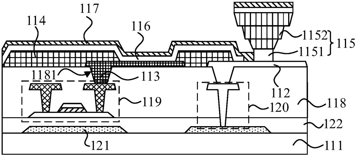
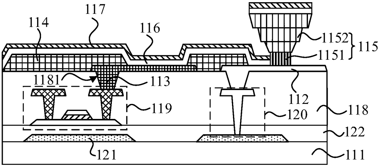
[0014] refer to figure 1 , figure 1 It is a schematic structural view of an embodiment of a display panel provided in this application, and the display panel includes: a substrate 111 , an auxiliary electrode 112 , an anode 113 , a pixel definition layer 114 , cathode isolation columns 115 , a light emitting layer 116 and a cathode 117 .

[0015] The substrate 111 can be a glass substrate or a resin substrate; the auxiliary electrode 112 and the anode 113 are...