Thermal compensation optical wave multiplexing and demultiplexing chip and preparation method thereof

A light wave multiplexing and demultiplexing technology, applied in the direction of optical waveguide, light guide, optics, etc., to achieve the effect of increasing polarization-dependent loss, increasing insertion loss uniformity, and realizing temperature drift compensation

Active Publication Date: 2019-02-26
苏州亿波达光电子科技有限公司
View PDF9 Cites 5 Cited by
  • Summary
  • Abstract
  • Description
  • Claims
  • Application Information

AI Technical Summary

Problems solved by technology

[0016] However, there are technical difficulties in this invention, that is, the input waveguide needs to be cut (fragmentation treatment), the precision machining of the mechanical compensation mechanism and the selection of materials used, and the control of the distance between the two input waveguides after cutting.

Method used


Image

  • Thermal compensation optical wave multiplexing and demultiplexing chip and preparation method thereof
  • Thermal compensation optical wave multiplexing and demultiplexing chip and preparation method thereof
  • Thermal compensation optical wave multiplexing and demultiplexing chip and preparation method thereof

Examples


Embodiment Construction

[0052] In order to better explain the present invention and facilitate understanding, the present invention will be described in detail below through specific embodiments in conjunction with the accompanying drawings.

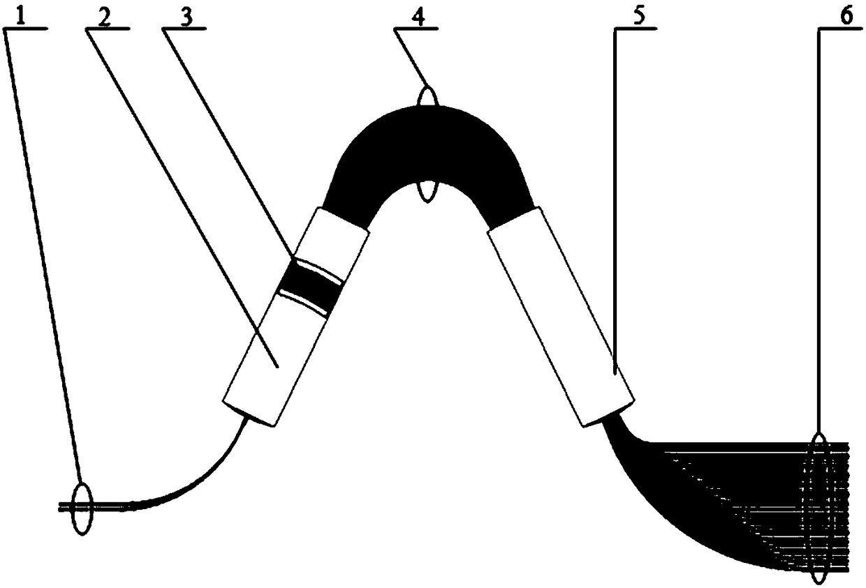
[0053] The invention provides a thermally compensated light wave multiplexing and demultiplexing chip, that is, a grating structure is etched at the input slab waveguide of the chip on the basis of , and the grating structure is filled with negative refraction for realizing the temperature drift compensation function High-efficiency materials, so that the light incident to the arrayed waveguide from the input slab waveguide of the chip does not drift with temperature.

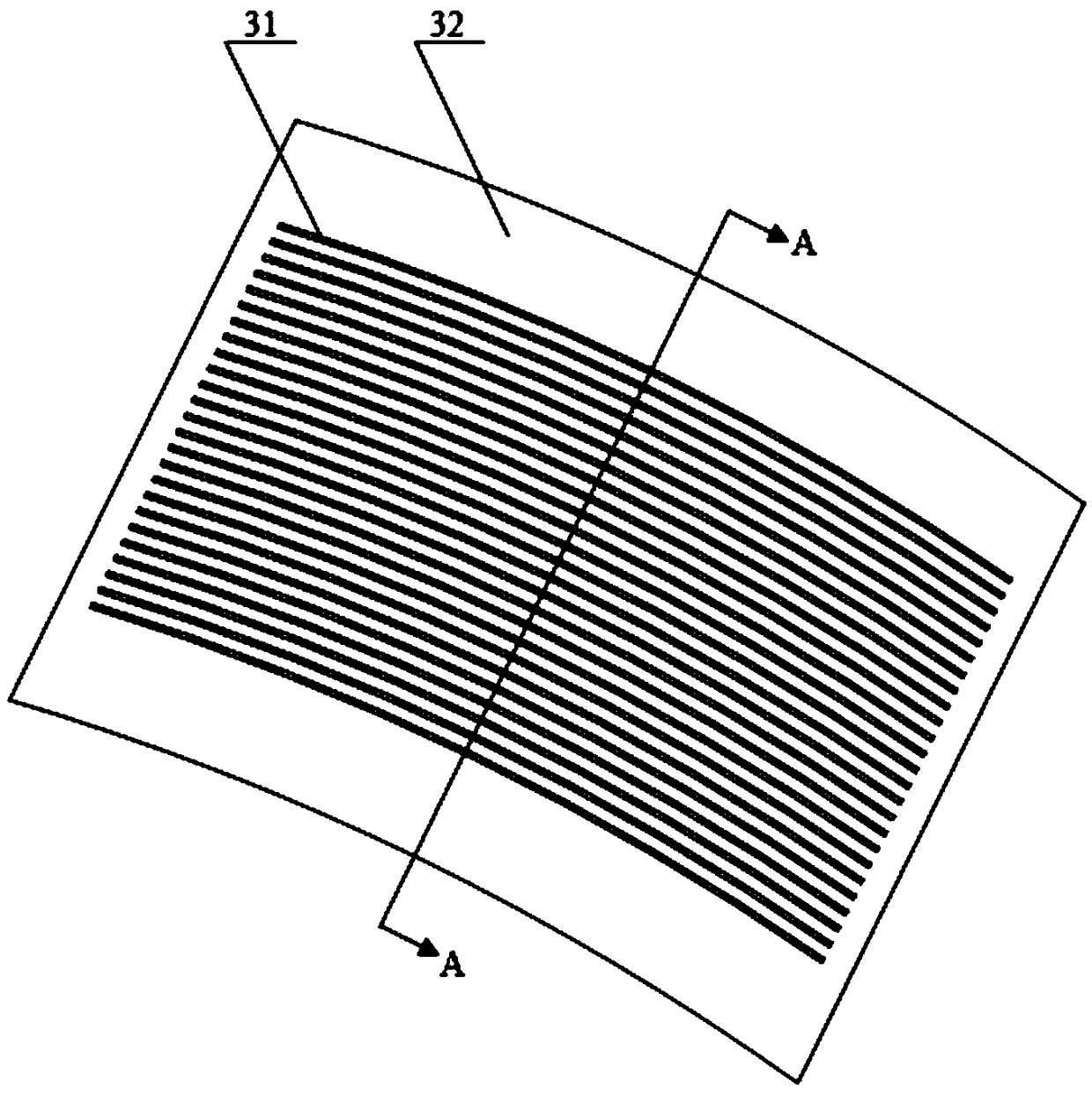
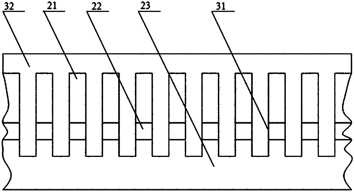
[0054] Specifically, a thermal compensation structure 3 is provided on the input star coupler 2, and the thermal compensation structure 3 includes a grooved grating 31, and the grooved grating 31 is filled with a negative refractive index material for realizing the temperature drift compensation fu...


PUM


Abstract

The invention relates to the technical field of optical wavelength division multiplexing, and in particular relates to a thermal compensation optical wave multiplexing and demultiplexing chip and a preparation method thereof. The thermal compensation optical wave multiplexing and demultiplexing chip provided by the invention comprises an input array waveguide, an input star coupler, an array waveguide, an output star coupler and an output array waveguide; a thermal compensation structure is arranged on the input star coupler, and a trench grating is processed through a semiconductor process; and negative thermal expansion coefficient silica gel is filled in the trench grating. According to the thermal compensation optical wave multiplexing and demultiplexing chip and the preparation methodthereof, the grating structure is etched on the input star coupler and is filled with a negative refractive index material to achieve temperature drift compensation; and the chip is free of stress control and fragmentation, and has the advantages of easy integration manufacture, compact structure, low transmission loss, uniform insertion loss, low polarization-dependent loss and the like.

Description

technical field [0001] The invention relates to the technical field of optical wavelength division multiplexing, in particular to a thermally compensated optical wave multiplexing and demultiplexing chip and a preparation method thereof. Background technique [0002] With the rapid development of technologies such as big data, cloud storage and computing, 5th generation mobile communication, Internet of Things, virtual reality and artificial intelligence, as the basis of information transmission, optical fiber communication system is still the bottleneck of the development of new generation information technology. As the basis of the optical fiber communication system, the development level of the optical communication device is the bottleneck in the development of the new generation of information technology, especially the optical multiplexer and demultiplexer, which is necessary to form a high-speed, large-capacity, intelligent optical fiber communication system. . [00...

Claims


Application Information

Patent Timeline
Patent Type & Authority Applications(China)
IPC IPC(8): G02B6/12
CPCG02B6/12028
Inventor 郑煜吴雄辉郜飘飘段吉安
Owner 苏州亿波达光电子科技有限公司
Why Eureka
Try Eureka