Semiconductor device manufacturing method and adhesive laminate

A manufacturing method and semiconductor technology, which is applied in semiconductor/solid-state device manufacturing, semiconductor devices, semiconductor/solid-state device components, etc., can solve the problem of low adhesion and achieve the effect of high functionality

Pending Publication Date: 2019-02-26
LINTEC CORP
View PDF8 Cites 2 Cited by
  • Summary
  • Abstract
  • Description
  • Claims
  • Application Information

AI Technical Summary

Problems solved by technology

[0004] However, the adhesive tape described in Document 1 is a temporary fixing tape, so the adhesive force is low, and there is a possibility that the chip may be displaced from the designated position due to the pressure during resin sealing.

Method used


Image

  • Semiconductor device manufacturing method and adhesive laminate
  • Semiconductor device manufacturing method and adhesive laminate
  • Semiconductor device manufacturing method and adhesive laminate

Examples


no. 1 Embodiment approach 〕

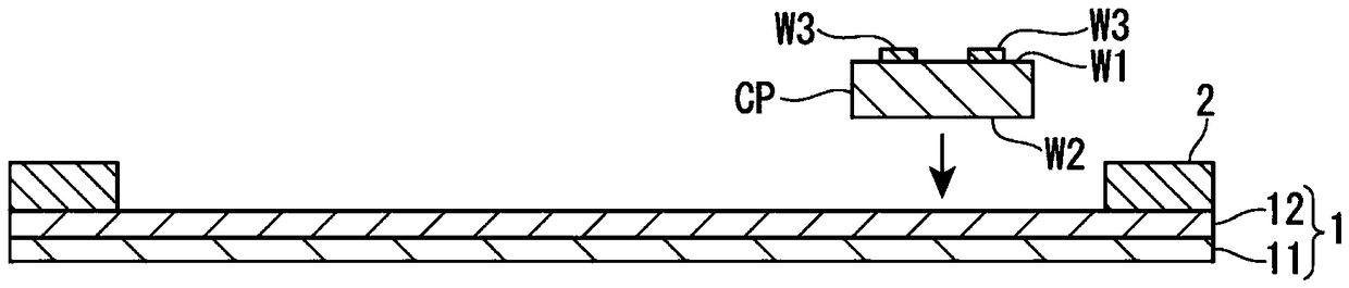
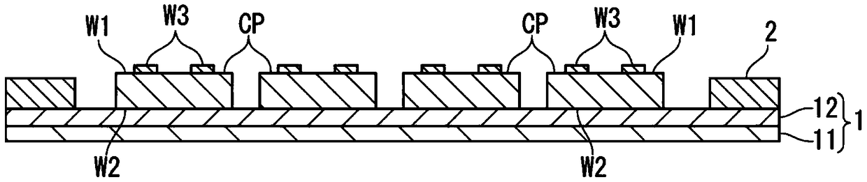
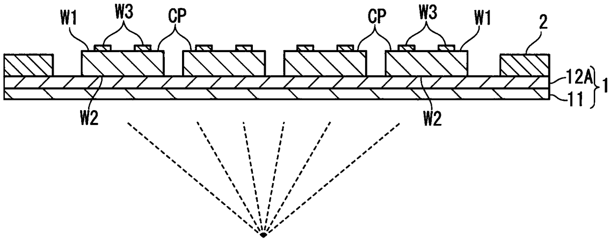
[0072] The manufacturing method of the semiconductor device according to this embodiment has the following steps: a step of affixing a plurality of semiconductor elements to the adhesive layer of the bonded laminate; a step of curing the adhesive layer to form a cured adhesive layer; A process of sealing a plurality of the above-mentioned semiconductor elements to form a sealing body having a sealing resin layer; a step of peeling the above-mentioned base material from the above-mentioned sealing body without peeling the above-mentioned cured adhesive layer from the above-mentioned sealing body; A step of rewiring layer for electrically connecting elements; and a step of electrically connecting external terminal electrodes to said rewiring layer, wherein when a plurality of said semiconductor elements are attached to said adhesive laminate, the said semiconductor element and the The back surface of the element on the opposite side of the circuit surface of the connection termin...

no. 2 Embodiment approach 〕

[0201] The manufacturing method of the semiconductor device according to this embodiment has the following steps: a step of affixing a plurality of semiconductor elements to the adhesive layer of the bonded laminate; a step of curing the adhesive layer to form a cured adhesive layer; A process of sealing a plurality of the above-mentioned semiconductor elements to form a sealing body having a sealing resin layer; a step of peeling the above-mentioned base material from the above-mentioned sealing body without peeling the above-mentioned cured adhesive layer from the above-mentioned sealing body; A step of rewiring layer for electrically connecting elements; a step of electrically connecting external terminal electrodes to said rewiring layer, wherein when a plurality of said semiconductor elements are attached to said adhesive laminated body, said semiconductor elements having connection terminals The circuit surface of the above-mentioned circuit surface is pasted toward the a...

no. 3 Embodiment approach 〕

[0362] The method of manufacturing a semiconductor device according to this embodiment is a method of manufacturing an adhesive laminate including a base material and an adhesive layer, and further comprising an adhesive layer between the adhesive layer and the base material. mixture layer. The manufacturing method of the semiconductor device of this embodiment has the following steps: the step of affixing a plurality of semiconductor elements to the above-mentioned adhesive layer of such an adhesive laminate; and the step of curing the above-mentioned adhesive layer to form a cured adhesive layer. A step; a step of sealing a plurality of the semiconductor elements to form a sealing body having a sealing resin layer; a step of peeling the base material from the sealing body without peeling the cured adhesive layer from the sealing body; forming a step of electrically connecting a rewiring layer to the semiconductor element; and a step of electrically connecting an external ter...


PUM

PropertyMeasurementUnit
thicknessaaaaaaaaaa
thicknessaaaaaaaaaa
glass transition temperatureaaaaaaaaaa

Abstract

The present invention provides semiconductor device manufacturing method, including a step of adhering a substrate (11) and a semiconductor element with an adhesive layer interposed therebetween; a step of curing the adhesive layer to form a cured adhesive layer (12A); a step of sealing the plurality of the semiconductor elements to form a sealed body (3) having a seal resin layer; a step of striping the substrate (11) from the sealed body (3) without stripping the cured adhesive layer (12A) from the sealed body (3); a step of forming a rewiring layer electrically connected to the semiconductor elements; and a step of electrically connecting an external terminal electrode and the rewiring layer.

Description

technical field [0001] The present invention relates to a method of manufacturing a semiconductor device and an adhesive laminate. Background technique [0002] In recent years, miniaturization, weight reduction, and higher functionality of electronic devices have been progressing. Semiconductor devices mounted in electronic equipment are also required to be smaller, thinner, and denser. Semiconductor chips (sometimes simply called chips) are sometimes mounted in packages close to their size. Such a package is sometimes called a chip scale package (Chip Scale Package; CSP). As one of the processes for manufacturing the CSP, wafer level packaging (Wafer Level Package; WLP) can be mentioned. In WLP, external electrodes and the like are formed on the chip circuit formation surface before the package is singulated by dicing, and finally the package wafer including the chip is diced and singulated. Examples of WLP include fan-in (Fan-In) type and fan-out (Fan-Out) type. In f...

Claims


Application Information

Patent Timeline
Patent Type & Authority Applications(China)
IPC IPC(8): H01L21/56H01L23/485C09J7/22C09J7/30C09J7/38C09J201/00C09J11/04C09J11/06
CPCH01L21/568H01L23/485C09J7/22C09J7/30C09J7/38C09J11/04C09J11/06C09J201/00C09J2203/326C09J2301/304C09J2301/302H01L2224/73267H01L2924/18162H01L2224/04105H01L2224/12105H01L2224/18H01L21/563H01L21/565H01L24/27H01L24/28H01L21/52
Inventor 冈本直也山田忠知菊池和浩
Owner LINTEC CORP
Why Eureka
Try Eureka