Novel 3D NAND memory device and method of forming same

A device and storage unit technology, applied in the field of three-dimensional storage devices and vertical 3DNAND storage devices, can solve the problems of complex manufacturing process of 3DNAND storage devices, and achieve the effect of reducing channel resistance

Active Publication Date: 2019-03-01
YANGTZE MEMORY TECH CO LTD
View PDF6 Cites 7 Cited by
  • Summary
  • Abstract
  • Description
  • Claims
  • Application Information

AI Technical Summary

Problems solved by technology

[0003] Compared with the planar transistor structure, the vertical structure of 3D NAND memory device involves more critical and complex manufacturing process
As 3D NAND memory devices move toward higher density configurations with more memory cell layers at a lower cost per bit, improvements to the structure and its fabrication methods become increasingly challenging

Method used


Image

  • Novel 3D NAND memory device and method of forming same
  • Novel 3D NAND memory device and method of forming same
  • Novel 3D NAND memory device and method of forming same

Examples


Embodiment Construction

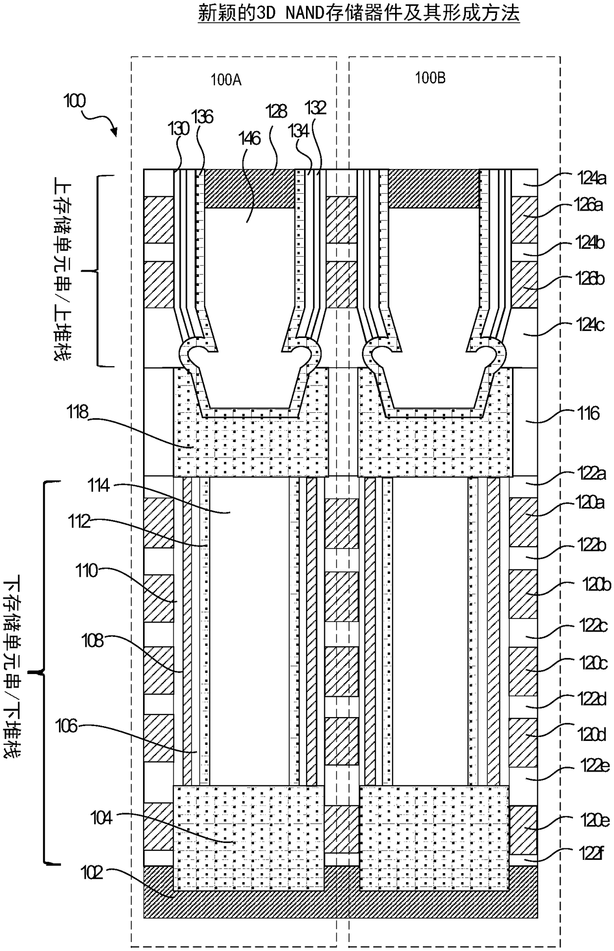
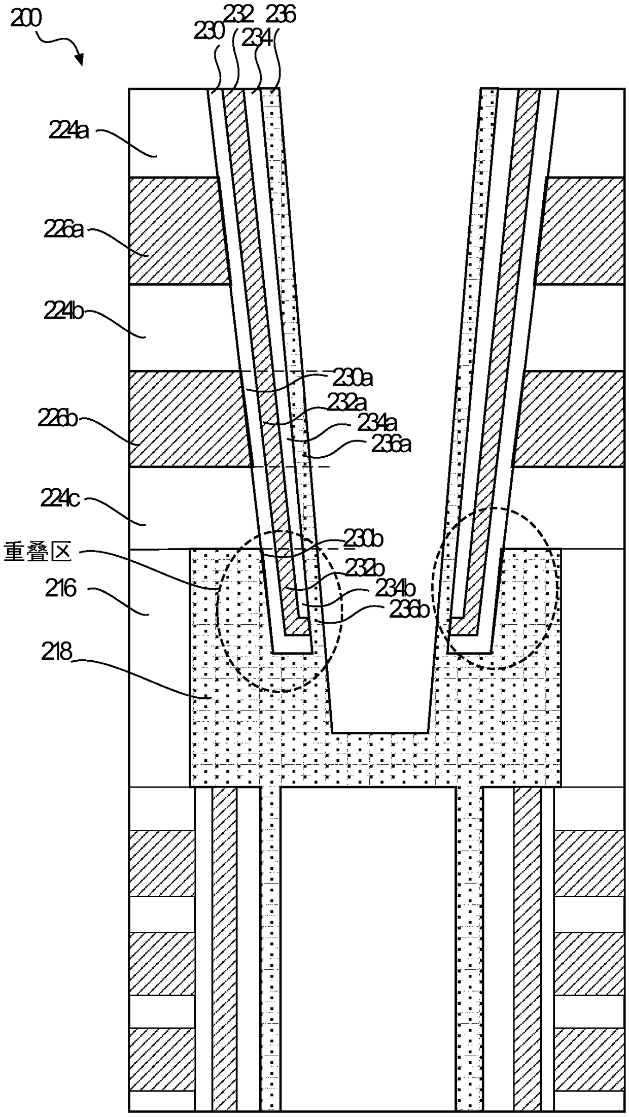
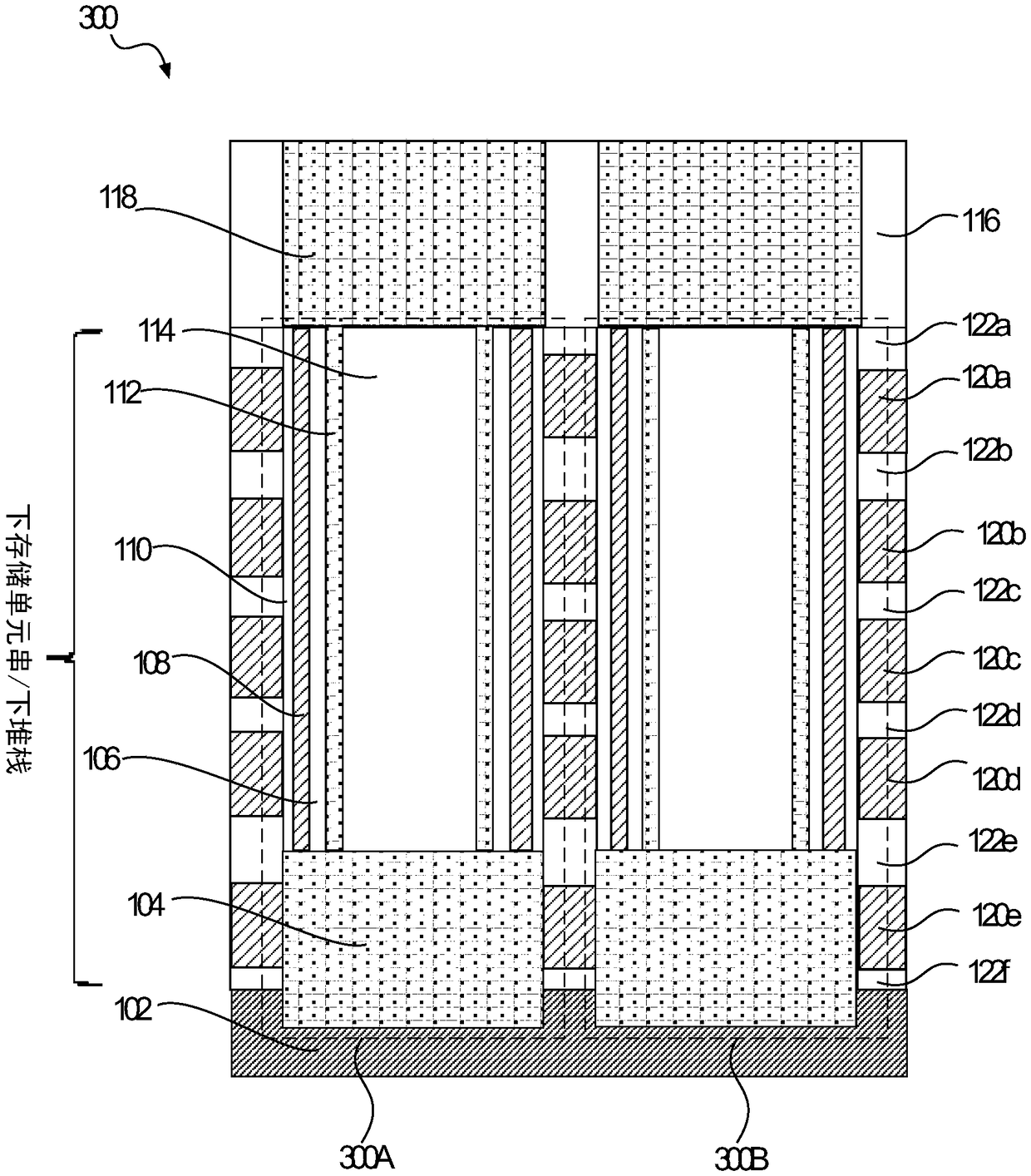
[0017] The following disclosure provides many different embodiments, or examples, for implementing different features of the presented subject matter. Specific examples of components and arrangements are described below to simplify the present disclosure. Of course, these are examples only and are not meant to be limiting. For example, forming a first feature on or over a second feature in the description below may include embodiments in which the first and second features are features that are formed in direct contact, and may also include embodiments in which the first feature and the second feature may be formed in direct contact. An embodiment in which an additional feature is formed between a first feature and a second feature such that the first feature and the second feature may not be in direct contact. Also, the present disclosure may reuse numbers and / or letters in reference numerals in various examples. This repetition is for the purposes of simplicity and clarity...


PUM


Abstract

In the memory device, a lower memory cell string including a first channel structure, a plurality of first word line layers, and a first insulating layer is formed over a substrate. The first channelstructure extends from the substrate and passes through the first word line layer and the first insulating layer. Inter-stack contacts are formed over the lower memory cell string and coupled to the first channel structure. An upper memory cell string is formed over the inter-stack contacts. The upper memory cell string includes a second channel structure, a plurality of second word lines, and a second insulating layer. The second channel structure passes through the second word line and the second insulating layer and extends into the inter-stack contacts and further laterally into the secondinsulating layer. A channel dielectric region of the second channel structure is above the inter-stack contacts.

Description

Background technique [0001] As the critical dimensions of devices in integrated circuits shrink to the limits of common memory cell technology, designers have been looking for ways to stack multiple planes of memory cells to achieve higher storage capacities and achieve lower cost-per-bit technology. [0002] The inventive concept relates to a nonvolatile memory device, and more particularly to a vertical type 3D NAND memory device in which a channel structure extends in a vertical direction. As the size of electronic products can be gradually reduced, these products may be required to perform data processing at a higher capacity. Accordingly, the degree of integration of semiconductor memory devices used in electronic products can be increased. A method of increasing the integration of semiconductor memory devices may involve nonvolatile memory devices having a vertical structure instead of a planar transistor structure. [0003] Compared with the planar transistor structu...

Claims


Application Information

Patent Timeline
Patent Type & Authority Applications(China)
IPC IPC(8): H01L27/1157H01L27/11575H01L27/11582
CPCH10B43/35H10B43/50H10B43/27G11C5/063H10B41/27H10B41/35
Inventor 张若芳王恩博杨号号徐前兵胡禺石张富山
Owner YANGTZE MEMORY TECH CO LTD
Why Eureka
Try Eureka