Laser annealing device and surface resistance calculation device

A technology of surface resistance and laser annealing, which is applied in the direction of measuring devices, circuits, measuring electronics, etc., can solve the problems of semiconductor wafer damage, time-consuming and labor-intensive problems

Active Publication Date: 2022-04-08
SUMITOMO HEAVY IND LTD
View PDF11 Cites 0 Cited by
  • Summary
  • Abstract
  • Description
  • Claims
  • Application Information

AI Technical Summary

Problems solved by technology

Therefore, the measurement of surface resistance becomes an offline operation, which is time-consuming and labor-intensive.
Also, since the probes must be brought into contact with the semiconductor wafer, the semiconductor wafer can be damaged

Method used


Image

  • Laser annealing device and surface resistance calculation device
  • Laser annealing device and surface resistance calculation device
  • Laser annealing device and surface resistance calculation device

Examples


Embodiment Construction

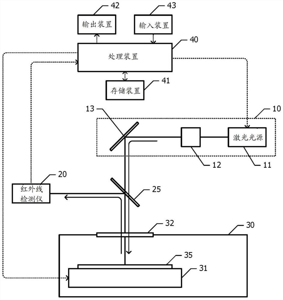
[0022] Below, refer to Figure 1 ~ Figure 5C , the laser annealing apparatus based on the embodiment will be described.

[0023] figure 1 It is a schematic diagram of the laser annealing apparatus based on an Example. The laser annealing device based on the embodiment includes a laser optical system 10 , a chamber 30 , an infrared detector 20 , a processing device 40 , a storage device 41 , an output device 42 and an input device 43 .

[0024] The laser optical system 10 includes a laser light source 11 , a homogenizing optical system 12 and a turning mirror 13 . The laser light source 11 outputs a laser beam in an infrared region. As the laser light source 11, for example, a laser diode with an oscillation wavelength of 808 nm can be used. The homogenizing optical system 12 homogenizes the beam distribution of the laser beam output from the laser light source 11 . The turning mirror 13 reflects the laser beam passing through the homogenizing optical system 12 downward. ...


PUM

PropertyMeasurementUnit
lengthaaaaaaaaaa
widthaaaaaaaaaa

Abstract

The present invention provides a laser annealing device capable of reducing the man-hours for measuring surface resistance and measuring surface resistance in a non-contact manner. A semiconductor wafer is held on the stage. A laser beam is incident on a semiconductor wafer held on a stage from a laser optical system. Thermal radiant light from a semiconductor wafer held on a stage is incident on an infrared detector. The infrared detector outputs a signal corresponding to the intensity of the thermal radiation light. The processing device calculates the surface resistance of the semiconductor wafer annealed by the laser beam according to the output value of the infrared detector, and outputs the calculated value of the surface resistance to the output device.

Description

[0001] This application claims priority based on Japanese Patent Application No. 2017-170504 filed on September 5, 2017. The entire contents of this Japanese application are incorporated herein by reference. technical field [0002] The invention relates to a laser annealing device and a surface resistance calculation device. Background technique [0003] Conventionally, sheet resistance has been measured as an example of a method for grasping the in-plane distribution of the activation state of a semiconductor wafer implanted with a dopant and subjected to activation annealing. The activation state of the dopant can be evaluated from the in-plane distribution of the surface resistance. [0004] Patent Document 1: Japanese Patent Laid-Open No. 2007-81348 [0005] Generally, a four-probe method is used in the measurement of surface resistance. The measurement of surface resistance using the four-probe method was performed after annealing in a device different from the acti...

Claims


Application Information

Patent Timeline
Patent Type & Authority Patents(China)
IPC IPC(8): H01L21/67H01L21/66
CPCH01L21/67115H01L22/14H01L22/20G01J5/20G01R31/2831H01L21/268H01L21/324
Inventor 田中哲平
Owner SUMITOMO HEAVY IND LTD
Why Eureka
Try Eureka