Circuit board and manufacturing method thereof

A manufacturing method and circuit board technology, applied to printed circuits, printed circuits, printed circuit components, etc., can solve the problems of nickel layer corrosion, gold layer peeling off, nickel layer corrosion, etc., to reduce the contact area and prevent peeling The effect of shedding and delaying the reaction time

Active Publication Date: 2020-12-15
HONGQISHENG PRECISION ELECTRONICS (QINHUANGDAO) CO LTD +1
View PDF5 Cites 0 Cited by
  • Summary
  • Abstract
  • Description
  • Claims
  • Application Information

AI Technical Summary

Problems solved by technology

When the circuit board is working in a humid and high-temperature environment, corrosive gases will enter through the tiny gaps, and the galvanic effect is likely to occur at the junction of the nickel-plated layer and the gold-plated layer to corrode the nickel-plated layer , the final result is that the nickel layer is gradually corroded, and the gold layer is peeled off. When the nickel layer has a void, the galvanic corrosion between the nickel layer and the copper conductive circuit layer occurs, so the nickel layer may be completely corroded.

Method used


Image

  • Circuit board and manufacturing method thereof
  • Circuit board and manufacturing method thereof
  • Circuit board and manufacturing method thereof

Examples


no. 1 example

[0050] Taking the manufacture of a single-layer circuit board as an example below, the method for manufacturing the circuit board 100 provided by the technical solution will be described. The method for manufacturing the circuit board 100 includes the following steps:

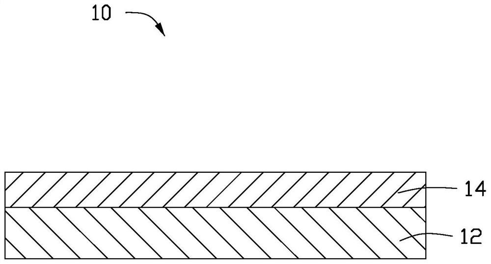
[0051] For step S1, see figure 1 , providing a copper-clad substrate 10, the copper-clad substrate 10 is a single-sided copper-clad substrate. The copper-clad substrate 10 may be a flexible copper-clad substrate or a rigid copper-clad substrate. The copper-clad substrate 10 includes an insulating layer 12 and a copper foil layer 14 formed on the surface of the insulating layer 12, and the thickness of the copper foil layer 14 may be 2um.

[0052] In other embodiments, the copper-clad substrate 10 may also be a double-layer copper-clad substrate.

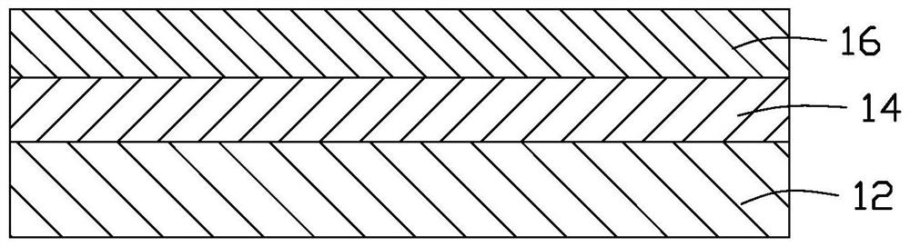
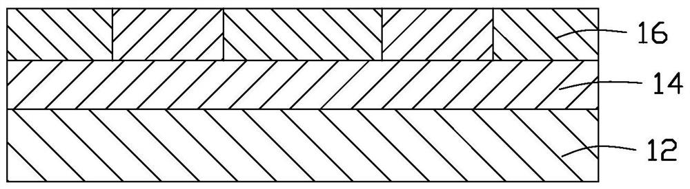
[0053] In the second step S2, please refer to Figure 2-6 , forming the copper foil layer 14 into a conductive structure. The conductive structure 14 includes a p...

no. 2 example

[0071] see Figure 9 The circuit board 200 provided by the second embodiment is basically the same as the circuit board 100 provided by the first embodiment, the difference is that the cross-sectional shape of the protruding edge 244 of the circuit board 200 is a rectangle, and the protruding edge 244 The height is less than the height of the quadrilateral 142 .

[0072] It can be understood that the conductive structure 14 of the circuit board 200 can be formed by two etching processes.

no. 3 example

[0074] see Figure 10 The circuit board 300 provided by the third embodiment is basically the same as the circuit board 100 provided by the first embodiment, except that the cross-sectional shape of the protruding edge 344 of the circuit board 300 is trapezoidal, and the height of the protruding edge 344 is less than the height of the quadrilateral 142 .

[0075] It can be understood that the conductive structure 14 of the circuit board 300 can be formed by two etching processes.


PUM


Abstract

The invention relates to a circuit board, which comprises an insulating layer, a conductive structure formed on the surface of the insulating layer, a nickel plating layer formed on the upper surface and side surfaces of the conductive structure, and a nickel plating layer formed on the upper surface and side surfaces of the nickel plating layer. A gold layer, the conductive structure includes a plurality of conductive patterns, the conductive pattern includes a quadrangle whose upper base length is equal to the lower base length and a protruding edge located at least on one side of the quadrangle, and the height of the protruding edge is less than or equal to The height of the quadrilateral. The present invention also provides a manufacturing method of the above-mentioned circuit board.

Description

technical field [0001] The invention relates to the field of circuit board production, in particular to a circuit board for preventing corrosive gas corrosion and a production method thereof. Background technique [0002] During the formation of the circuit board, after the formation of the copper conductive circuit layer, it is usually necessary to perform surface treatment on the copper conductive circuit layer to prevent oxidation of the copper conductive circuit layer. One of the most commonly used surface treatment methods is to form a nickel-plated layer on the surface of the copper conductive circuit layer and then form a layer of gold-plated layer on the surface of the nickel-plated layer. The nickel-plated layer covers the surface and sides of the copper conductive circuit layer, and the gold-plated layer covers the surface and side surfaces of the nickel-plated layer. Since the nickel-plated layer formed on the side of the copper conductive circuit layer relies on ...

Claims


Application Information

Patent Timeline
Patent Type & Authority Patents(China)
IPC IPC(8): H05K1/11H05K3/06
CPCH05K1/11H05K3/06H05K2201/09218
Inventor 侯宁何四红李彪黄美华
Owner HONGQISHENG PRECISION ELECTRONICS (QINHUANGDAO) CO LTD
Why Eureka
Try Eureka