Atomization assisting CVD thin film deposition method

A thin-film deposition and thin-film deposition device technology, applied in the field of atomization-assisted CVD thin-film deposition, can solve problems such as inability to ensure consistent concentration of precursor solution, inability to ensure credible and repeatable process parameters of film composition, and inability to avoid precursor reactions.

Active Publication Date: 2019-03-08
CHONGQING UNIV OF TECH +1
View PDF5 Cites 8 Cited by
  • Summary
  • Abstract
  • Description
  • Claims
  • Application Information

AI Technical Summary

Problems solved by technology

[0005] 1. The precursor used in CVD is a gas phase. Now there are more academic opinions that the CVD method cannot be directly mixed with a liquid aerosol precursor. In actual use, it is rare to have a liquid phase precursor material input.
[0006] 2. Pyrolytic spraying generally configures the precursor as a solution or a mixed solution and then puts it into the atomization source. After the atomization source is atomized into an aerosol, the liquid aerosol is input into the reaction chamber and pyrolysis occurs in the reaction area, so that The concentration of each component of the precursor cannot be guaranteed, nor can the precursor react in advance, so that the concentration of the precursor solution cannot be guaranteed to be consiste

Method used


Image

  • Atomization assisting CVD thin film deposition method
  • Atomization assisting CVD thin film deposition method
  • Atomization assisting CVD thin film deposition method

Examples


Embodiment Construction

[0044] Below in conjunction with accompanying drawing and embodiment the present invention will be further described:

[0045] A method for atomizing assisted CVD film deposition, characterized in that it comprises the steps of:

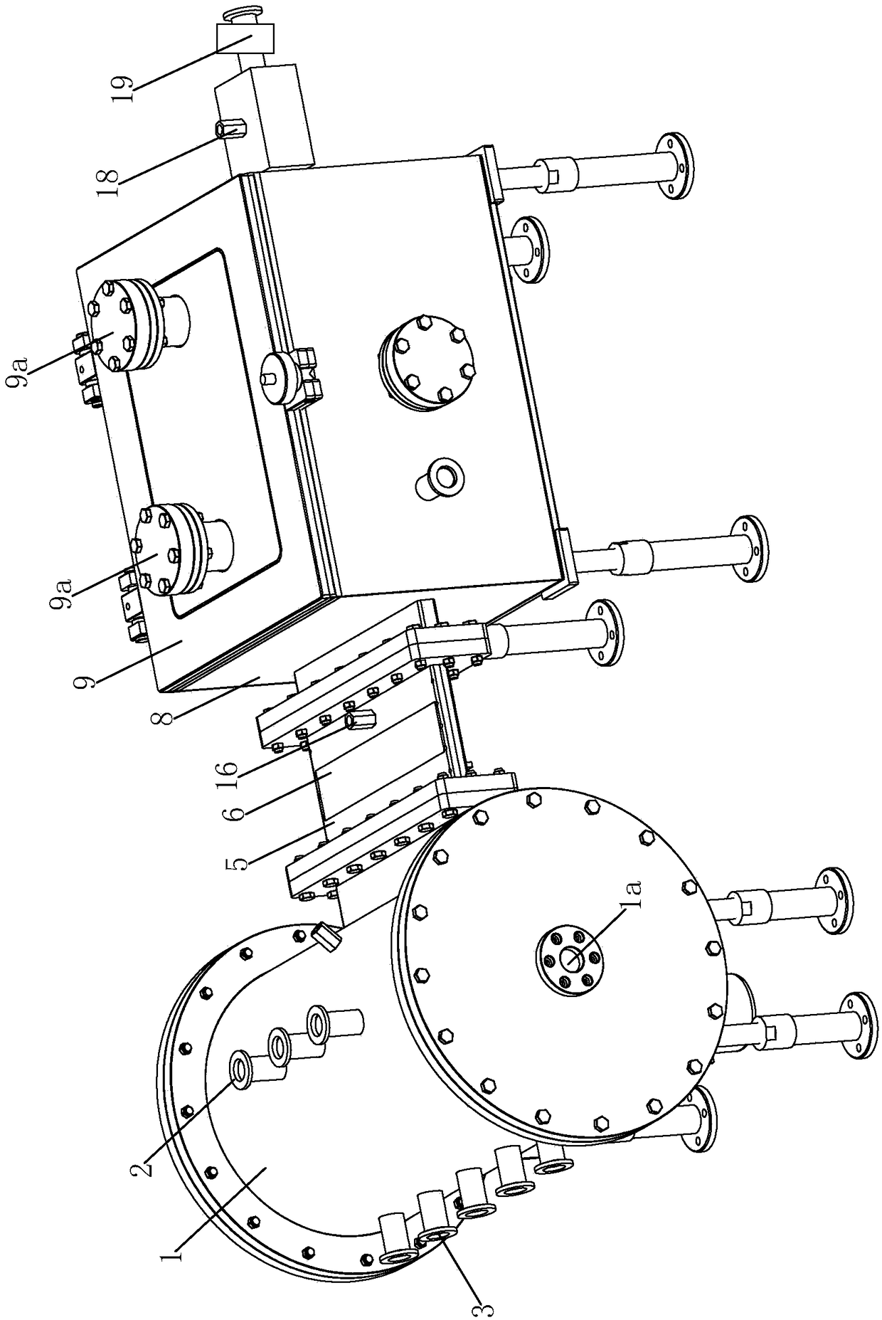
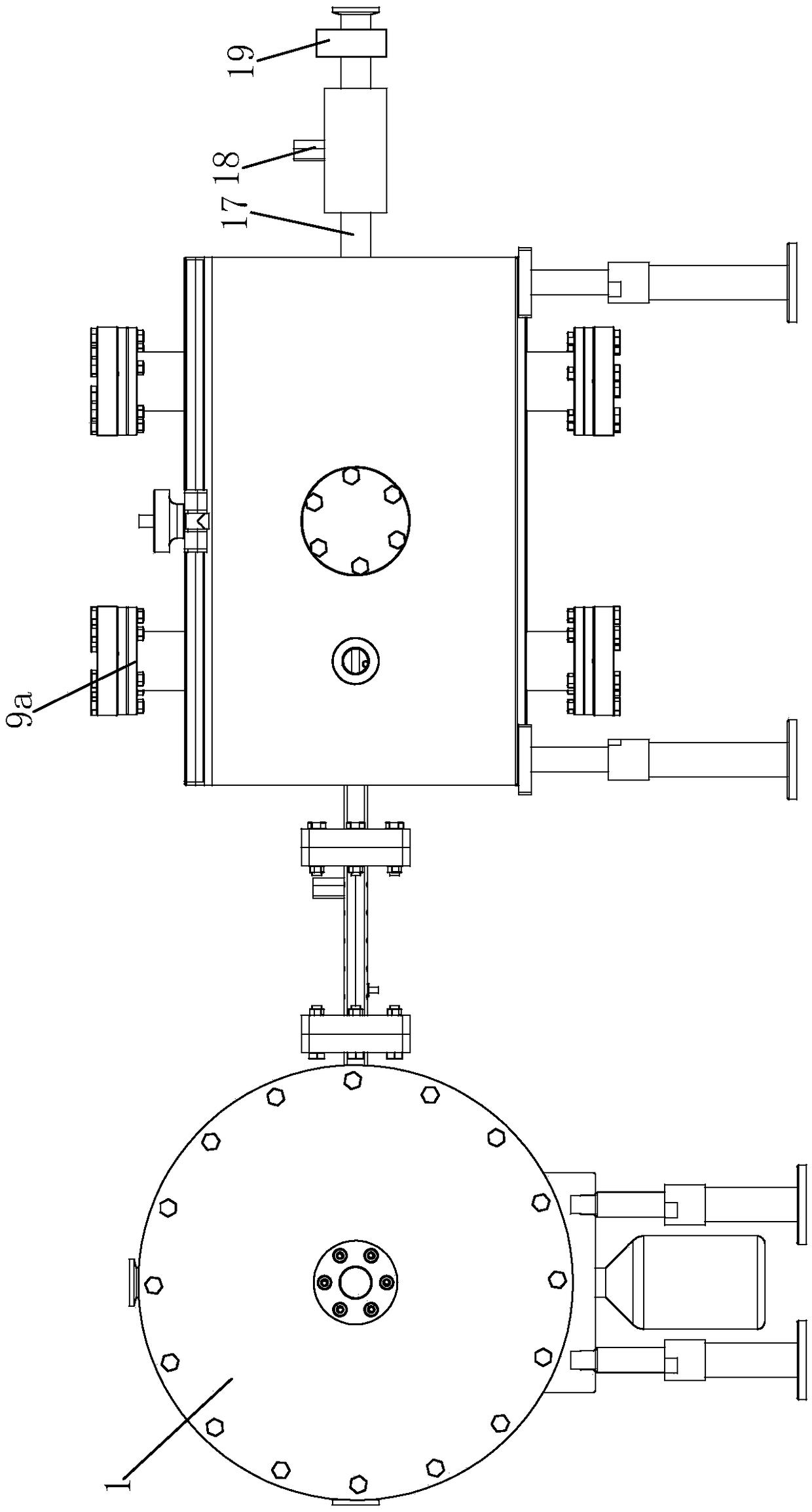
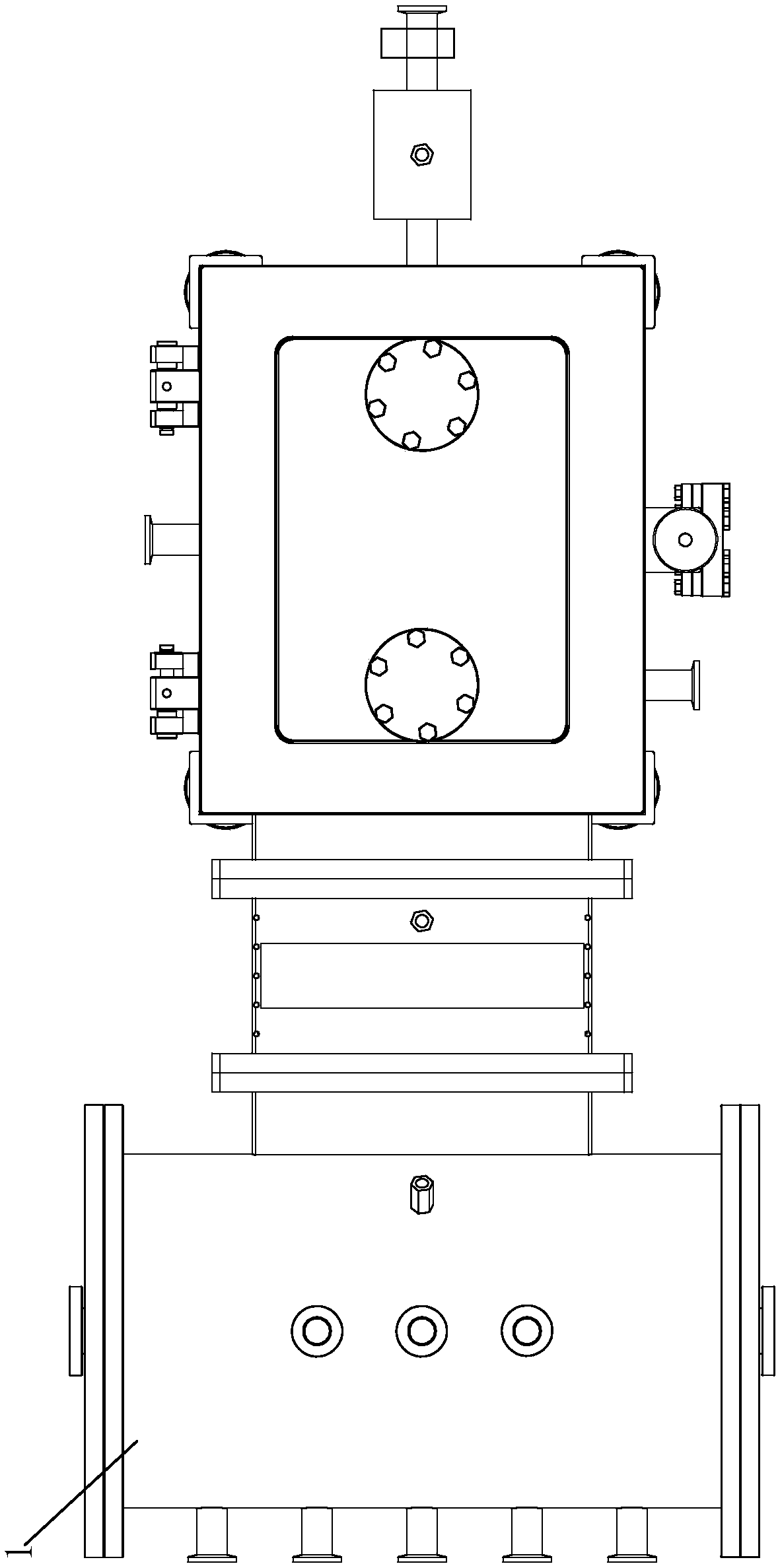
[0046] Step a: Design an atomization-assisted CVD film deposition device, such as Figure 1-5 As shown, an atomization-assisted CVD film deposition method mainly consists of three parts including a buffer mixing chamber 1 , a transition chamber 5 and a reaction chamber 8 . Wherein, the buffer mixing chamber 1 is made of corrosion-resistant material, preferably stainless steel. The top of the buffer mixing chamber 1 is vertically provided with multiple gas-phase material inlet pipes 2. In this case, the number of gas-phase material inlet pipes 2 is three, and they are arranged side by side. In mixing chamber 1. The left side of the buffer mixing chamber wall is provided with multiple aerosol inlet pipes 3. In this case, the number of aerosol inlet ...


PUM


Abstract

The invention discloses an atomization assisting CVD thin film deposition method. The atomization assisting CVD thin film deposition method is characterized by comprising the following steps that a, an atomization assisting CVD thin film deposition device is designed; b, a plane substrate being about to form a film is placed in an installing hole in a substrate template, then the substrate template is horizontally placed on the upper plate face of a lower lifting plate, and the position of the lower lifting plate is adjusted; d, after a temperature of a reaction area reaches a preset temperature, firstly an atomization source is opened, and is used for atomizing liquid precursors into aerosol precursors, the aerosol precursors are input into a buffering mixing chamber through carrier gas sent out of the atomization source; and e, after the temperature of the reaction area is close to a room temperature or is 45 DEG C or below, the operation that the precursors are input into the buffering mixing chamber through a gas phase matter inflow pipe and an aerosol inflow pipe firstly stops, then a gas sucking pump is closed, finally, a sealing cover is opened, the substrate template is taken out, and finally a substrate is taken down from the substrate template. The thin film deposition method is high in deposition efficiency, reasonable in process arrangement and high in thin film quality.

Description

technical field [0001] The invention belongs to the field of film preparation, in particular to an atomization-assisted CVD film deposition method. Background technique [0002] Thin film materials have a wide range of uses. The existing coating methods mainly include chemical vapor deposition (referred to as CVD) and physical vapor deposition (abbreviated as PVD). There are many sub-categories of coating methods. At present, the precursor of the conventional CVD deposition method is an all-gas phase substance, which is input into the reaction zone of the reaction device to undergo a chemical reaction after being heated or excited by other physical fields, and deposited on the substrate surface, and the CVD method is suitable for preparing high-quality thin films , but the cost is high, the film deposition speed is slow, and most CVD processes need to be carried out in a vacuum environment. The substrate has various structures, such as planar substrate and non-planar subst...

Claims


Application Information

Patent Timeline
IPC IPC(8): C23C16/455C23C16/448C23C16/40C23C18/12
CPCC23C16/40C23C16/4486C23C16/455C23C18/1216C23C18/1258
Inventor 龚恒翔冯倩郝跃廖飞杨专青马五吉
Owner CHONGQING UNIV OF TECH
Why Eureka
Try Eureka