Primary winding resonance wave trough sampling circuit and sampling method
A primary winding and sampling circuit technology, applied in electrical components, regulating electrical variables, high-efficiency power electronic conversion, etc., can solve the problems of increasing the volume of the transformer, increasing the cost, and the technical solution cannot meet this requirement, and achieves reduction in use and reduction. Small turn-off loss and volume reduction effect
- Summary
- Abstract
- Description
- Claims
- Application Information
AI Technical Summary
Problems solved by technology
Method used
Image

Examples
no. 1 example
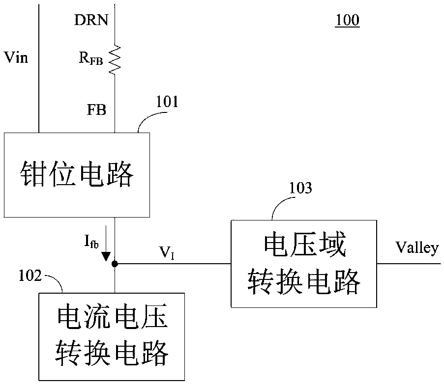
[0048] The first embodiment consists of Figure 5 The specific circuit diagram of the clamping circuit 101, Image 6 is a specific circuit diagram of the current-voltage conversion circuit 102, and Figure 7 The specific circuit diagram of the voltage domain conversion circuit 103 is realized.
[0049] The following is based on Figure 5 The 101 module circuit, Image 6 The 102 module circuit and Figure 7 The circuit analysis and theoretical calculation of the trough sampling process are given in the 103 module circuit.
[0050] Such as Figure 5 The module circuit shown in 101 includes PMOS transistors PM1, PM2, PM3, and NMOS transistors NM1, NM2. The source of PM1 is connected to the input voltage V in Connection, the gate and drain are connected to the gate of PM2, the gate of PM3, and the drain of NM1; the source of PM2 is connected to the source of FB and PM3, and the drain is connected to the gate of NM1, the gate of NM2 and The drain is connected; the source of...
no. 2 example
[0092] Figure 8 A schematic circuit diagram of the voltage domain conversion circuit 103 in the second embodiment shown. with the first embodiment Figure 7 The difference in the circuit schematic diagram of the voltage domain conversion circuit 103 shown is that Figure 7 The NMOS transistors N1, N2 and N3 are in Figure 8 are replaced by transistors T1, T2 and T3 respectively. The collector of transistor T1 and the bias current source I B connected at one end, I B The current flows to T1, the collector of T1 is also connected to the base of T1 and the base of T2, and the emitter of T1 is connected to the reference ground. The collector of T2 is connected to the drain of P1, the gate of P1, and the gate of P2, and the emitter of T2 is connected to the reference ground. T1 and T2 form a current mirror with a mirror ratio of k1. The collector of T3 is connected to the drain of P2 and the input of Schmitt trigger 201 to form the Va node, and the base of T3 and image 3 V...
PUM
 Abstract
Description
Claims
Application Information