Test method and test circuit for semiconductor sheet resistance

A technology of sheet resistance and test method, applied in the direction of measuring resistance/reactance/impedance, measuring device, measuring electrical variables, etc., can solve problems such as inaccurate measurement results

Active Publication Date: 2020-09-15
GLOBAL ENERGY INTERCONNECTION RES INST CO LTD
View PDF7 Cites 0 Cited by
  • Summary
  • Abstract
  • Description
  • Claims
  • Application Information

AI Technical Summary

Problems solved by technology

[0007] In view of this, an embodiment of the present invention provides a semiconductor sheet resistance test method and a test circuit to solve the problem that the sheet resistance measured by the existing test method will be affected by the depletion layer and make the measurement result inaccurate.

Method used


Image

  • Test method and test circuit for semiconductor sheet resistance
  • Test method and test circuit for semiconductor sheet resistance
  • Test method and test circuit for semiconductor sheet resistance

Examples


Embodiment 1

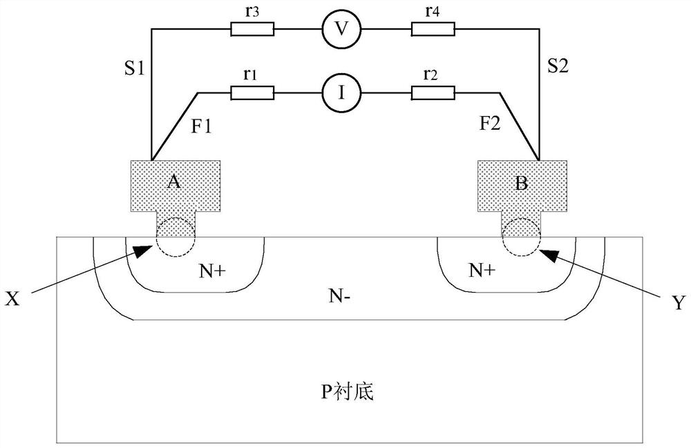
[0048] Figure 4A A schematic diagram of a test circuit for semiconductor sheet resistance according to an embodiment of the present invention is shown. Such as Figure 4A As shown, the doped region 11 to be tested is located in the semiconductor substrate 12 and is of the first conductivity type. At least one first doped region 13 is formed in the region 11 to be doped, and the first doped region 13 is of a second conductivity type, and the second conductivity type is opposite to the first conductivity type. A second doped region 14 is formed in the first doped region 13, and the second doped region is of the first conductivity type.

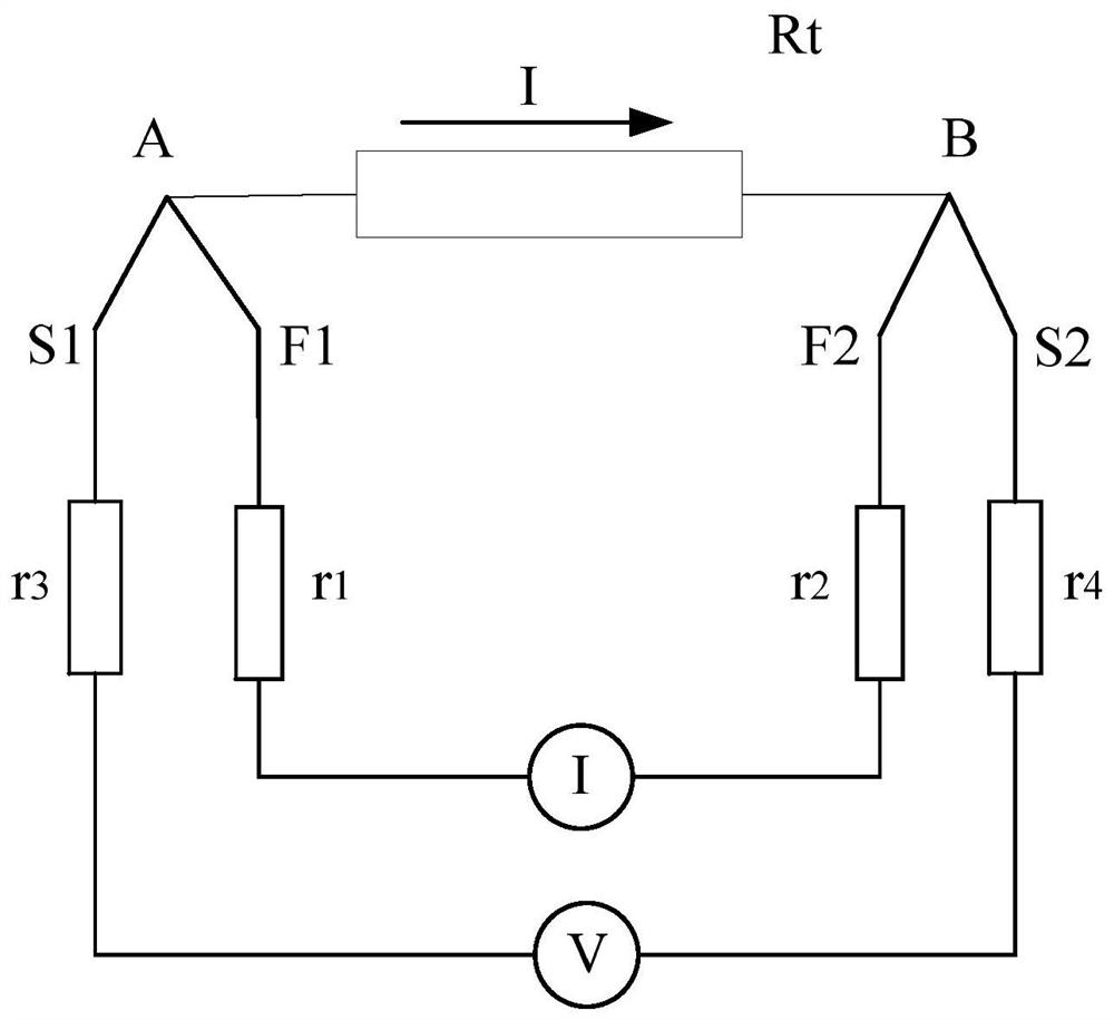
[0049] The testing circuit includes at least two excitation electrodes 21 and 22 , a DC power supply 30 , at least one isolation layer 41 and a corresponding control electrode 51 , at least two probes 61 and 62 , and a voltage measuring device 70 .

[0050] The positive and negative poles of the DC power supply 30 are respectively connected ...

Embodiment 2

[0058] Figure 5 A schematic diagram showing another semiconductor sheet resistance test circuit according to an embodiment of the present invention. Compare Figure 4A and Figure 5 It can be found that the test circuit differs from the first embodiment in that the ohmic contact region 15 is replaced by the first doped region 15 and the second doped region 16 , and also includes an isolation layer 42 and a control electrode 52 .

[0059] The first doped region 15 is located in the doped region 11 to be tested and is of the second conductivity type; the second doped region 16 is located in the first doped region 15 and is of the first conductivity type. The excitation electrode 21 corresponds to the second doped region 16 . The isolation layer 42 and the control electrode 52 are sequentially disposed on the surface of the semiconductor substrate 12 , and both extend from the edge of the first doped region 15 to the edge of the second doped region 16 inside the first doped r...

Embodiment 3

[0064] The embodiment of the present invention provides another test circuit for semiconductor sheet resistance, which differs from the first or second embodiment in that it also includes a processor connected to the DC power supply 30 and the voltage measuring device respectively to obtain test time The excitation current I and the voltage between the probes 61 and 62 are used to calculate the sheet resistance of the doped region 11 to be tested.


PUM


Abstract

The invention discloses a method and circuit for semiconductor square resistance. The method includes forming at least one first doping area in a to-be-tested doping area, wherein the first doping areas are in second conductivity types, and the second conductivity types are opposite to first conductivity types; forming second doping areas in the first doping areas, wherein the second doping areasare in the first conductivity types; arranging at least two excitation electrodes on the surface of a semiconductor substrate, wherein at least one excitation electrode is corresponding to the seconddoping areas; successively arranging at least one isolating layer and corresponding control electrodes on the surface of the semiconductor substrate, wherein the isolating layers and the control electrodes extend to the edge of the internal second doping area from the edge of one first doping area; applying excitation current through the two excitation electrodes, and testing the voltage of the to-be-tested doping area between the two excitation electrodes so that the square resistance value of the to-be-tested doping area can be obtained. Thus, accurate square resistance values can be obtained by performing square resistance tests through the method.

Description

technical field [0001] The invention relates to the technical field of semiconductor technology, in particular to a test method and a test circuit for semiconductor sheet resistance. Background technique [0002] Square resistance, also known as film resistance and surface resistance, refers to the resistance between the sides of a square thin film conductive material, which represents the compactness of the film layer. figure 1 A schematic diagram of a square film is shown, wherein a and b are the length and width of the square, a=b, and d is the thickness of the film. When the excitation current I is applied to the square film, and the flow direction of the current I is basically parallel to the surface of the film, according to the calculation formula of resistance, the square resistance can be obtained as It can be seen that the resistance of the square film is only related to the thickness and resistivity ρ of the square film, and has nothing to do with the length and...

Claims


Application Information

Patent Timeline
Patent Type & Authority Patents(China)
IPC IPC(8): G01R27/14
CPCG01R27/14
Inventor 王耀华金锐赵哿和峰刘钺杨曾军蒲奎杜文芳潘艳吴军民
Owner GLOBAL ENERGY INTERCONNECTION RES INST CO LTD
Why Eureka
Try Eureka