Display panel and mother board

A technology for display panels and motherboards, used in semiconductor/solid-state device parts, semiconductor devices, electrical components, etc., can solve problems such as the inability to place electrostatic short-circuit rings, and achieve the effect of improving electrostatic protection and eliminating static electricity.

Active Publication Date: 2019-03-08
KUNSHAN GO VISIONOX OPTO ELECTRONICS CO LTD
View PDF5 Cites 19 Cited by
  • Summary
  • Abstract
  • Description
  • Claims
  • Application Information

AI Technical Summary

Problems solved by technology

[0004] The present application provides a display panel and a display device, which can solve the problem in the prior art that the electrostatic short-circuit ring cannot be placed when the display panels are arranged at zero intervals in the motherboard.

Method used


Image

  • Display panel and mother board
  • Display panel and mother board
  • Display panel and mother board

Examples


Embodiment Construction

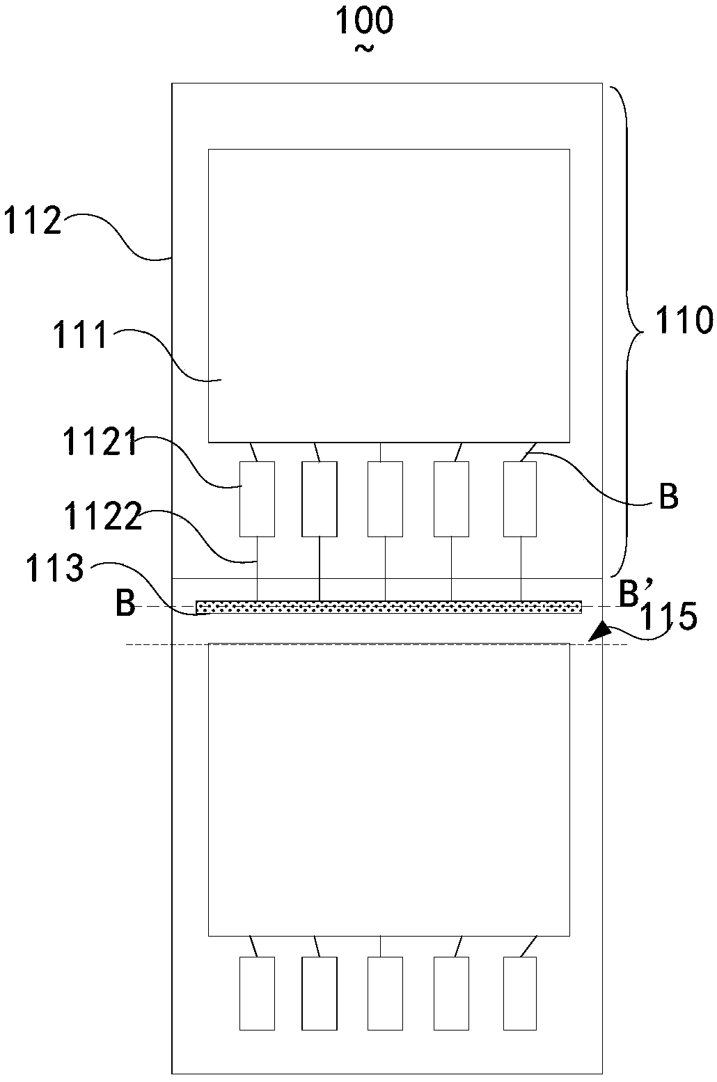
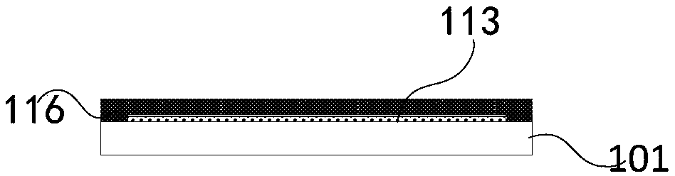
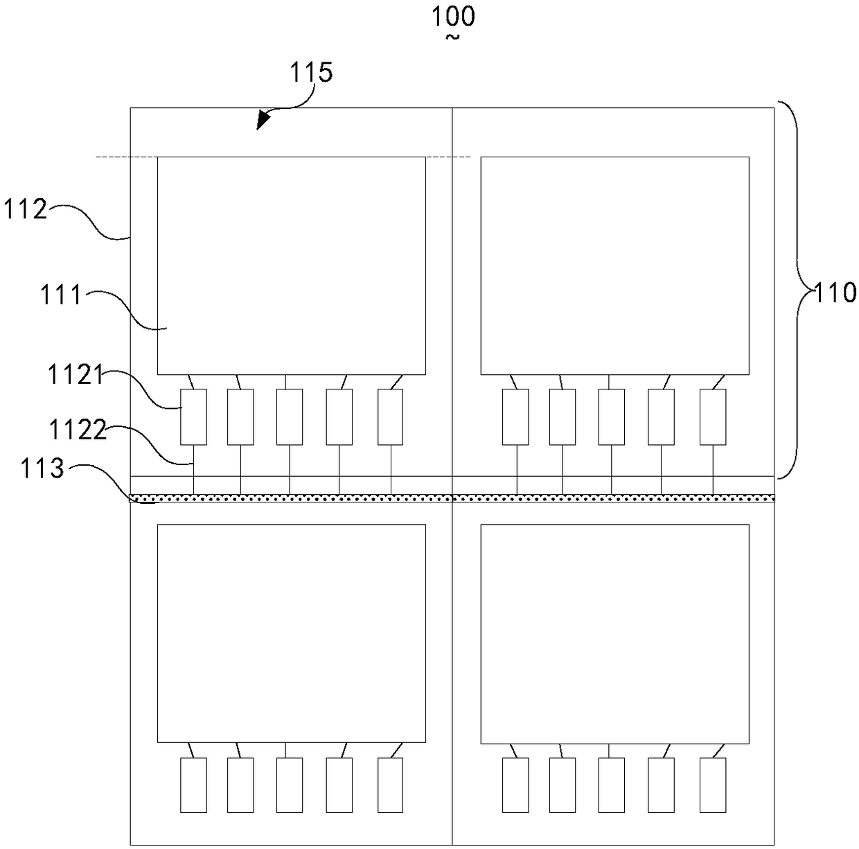
[0018] The following will clearly and completely describe the technical solutions in the embodiments of the present application with reference to the accompanying drawings in the embodiments of the present application. Obviously, the described embodiments are only part of the embodiments of the present application, not all of them. Based on the embodiments in this application, all other embodiments obtained by persons of ordinary skill in the art without making creative efforts belong to the scope of protection of this application.

[0019] The terms "first", "second", and "third" in this application are used for descriptive purposes only, and cannot be understood as indicating or implying relative importance or implicitly specifying the quantity of indicated technical features. Thus, features defined as "first", "second", and "third" may explicitly or implicitly include at least one of these features. In the description of the present application, "plurality" means at least t...


PUM


Abstract

The invention discloses a display panel and a mother board. The display panel mother board comprises a plurality of display panels arranged in an array mode; a display area and a non-display area on the periphery of the display area are defined on the surface of each display panel; each non-display area is provided with a plurality of conductive gaskets and a plurality of short-circuit connectinglines; an electrostatic short circuit ring is arranged on the non-display area of the display panel which is at least not in the first row; and one ends of the plurality of the short circuit connecting lines in each display panel in the same column are connected to the plurality of the conductive gaskets respectively, and the other ends of the short circuit connecting lines in each display panel are electrically connected with the electrostatic short circuit ring of the adjacent display panel in the next row. Therefore, static electricity generated for the display panels in a test or cutting process of the display panel mother board can be eliminated, and the electrostatic protection effect of the panels is improved.

Description

technical field [0001] The present application relates to the field of display technology, in particular to a display panel and a motherboard. Background technique [0002] Existing display panels are formed by cutting the display panel motherboard. Cutting lines are set on the display panel motherboard. The cutting lines divide the display panel motherboard into multiple display panel units. After the board is cut, one display panel unit corresponds to one display panel. [0003] Among them, in the process of making the display panel, in order to avoid the voltage difference between the signals and the large amount of static electricity generated by the mother board during cutting and testing, it is generally used to eliminate static electricity by connecting all signal lines at the same potential. influences. However, in order to realize the narrow bezel design, various conductive pads have been provided in the binding area of ​​the lower bezel of the display panel, and ...

Claims


Application Information

Patent Timeline
Patent Type & Authority Applications(China)
IPC IPC(8): H01L23/60H01L27/02
CPCH01L23/60H01L27/0292
Inventor 刘权张露王欢秦旭张金方胡思明韩珍珍
Owner KUNSHAN GO VISIONOX OPTO ELECTRONICS CO LTD
Why Eureka
Try Eureka