Array substrate motherboard, manufacturing method of array substrate motherboard and static electricity elimination device

A technology of an array substrate and a manufacturing method, which is applied in the field of an array substrate motherboard and its fabrication, and static elimination equipment, can solve problems such as affecting product quality, lead burning, and product yield decline.

Active Publication Date: 2015-04-29
HEFEI BOE OPTOELECTRONICS TECH +1
View PDF5 Cites 17 Cited by
  • Summary
  • Abstract
  • Description
  • Claims
  • Application Information

AI Technical Summary

Problems solved by technology

In this way, the static electricity generated during the rubbing alignment process, and a large amount of accumulated electrostatic charges will burn the lead wires, thereby seriously affecting the quality of the product and resulting in a decline in product yield

Method used


Image

  • Array substrate motherboard, manufacturing method of array substrate motherboard and static electricity elimination device
  • Array substrate motherboard, manufacturing method of array substrate motherboard and static electricity elimination device
  • Array substrate motherboard, manufacturing method of array substrate motherboard and static electricity elimination device

Examples


Embodiment 1

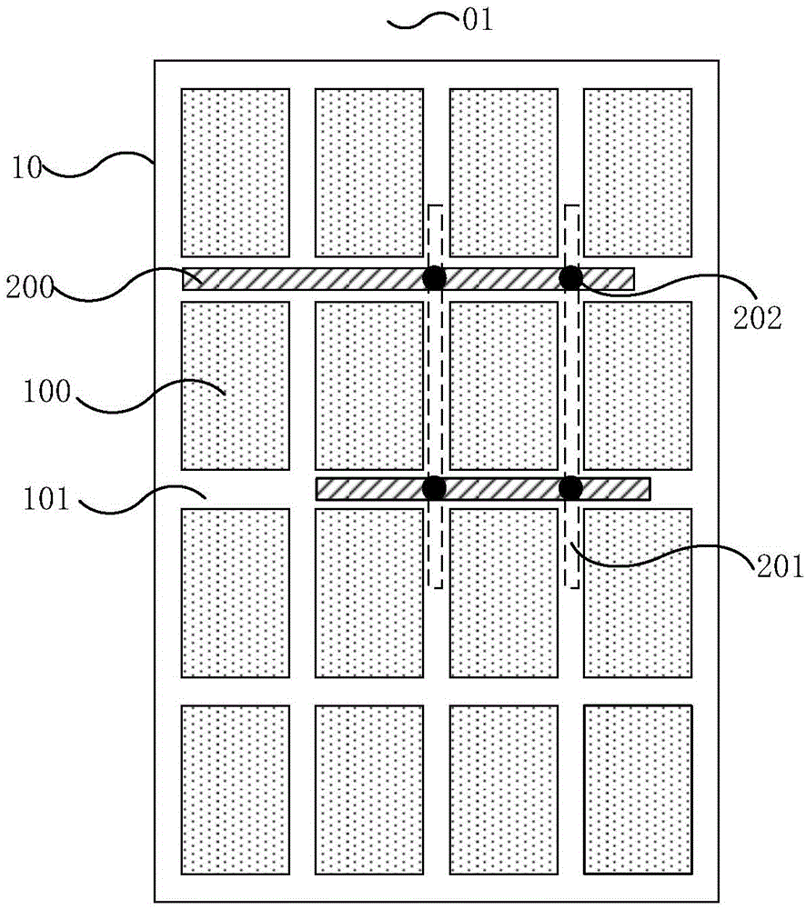
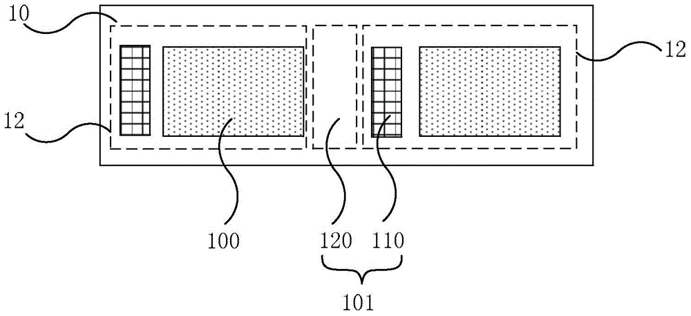
[0051] The non-display area 101 may include a binding area 110 and a gap area 120 between two adjacent display panels 12 , and the first wire 200 may be located in the gap area 120 .

[0052] Since the bonding area 110 is provided with a plurality of driving chips (gate driver 135 and source driver 134, etc.) interference, so the first wire 200 can be disposed in the gap region 120 . In addition, in the subsequent cutting process, the above-mentioned gap area 120 will be cut. If the line width of the first wire 200 is small, the first wire 200 arranged in the gap area 120 can be cut off together, so that the final There is no first wire 200 on the independent display panel 12 . This avoids signal interference caused by the existence of the first wire 200 during the display process of the display device.

[0053] In this case, the first wire 200 arranged in the gap area 120 can also be connected to the lead wire 13 in the binding area 110 or an electrostatic ring (not shown) ...

Embodiment 2

[0055] Since the size of the non-display area 101 between adjacent two display areas 100 is limited, in order to improve the effect of static electricity elimination, most of the space in the above-mentioned non-display area 101 can be covered by the first wire 200 to improve the first The contact area between the wire 200 and the rubbing cloth. However, if Figure 2a As shown, when the first conductive wire 200 with a certain line width is arranged obliquely in the above-mentioned non-display area 101 (the binding area 110 is omitted in the figure), it will not be able to cover most of the space in the non-display area 101 to the maximum extent. Therefore, if Figure 2b As shown, if the first wire 200 with a certain line width is arranged parallel to the 100 gate lines (or data lines) in the display area in the above-mentioned non-display area 101, it can occupy most of the space in the above-mentioned non-display area 101 , increase the contact area between the first wire ...

Embodiment 3

[0062] In the case that the non-display area 101 may include a bonding area 110 and a gap area 120 between two adjacent display panels 12, at least one lead wire 13 connected to a gate line or a data line in the binding area 110 as the first wire 200.

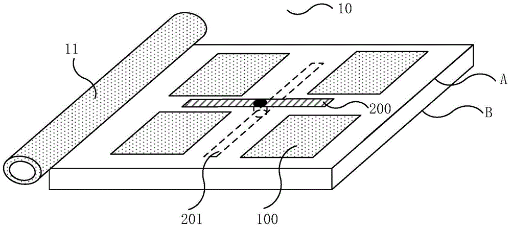
[0063] In this way, for the array substrate mother board 01 without the gap region 120 in the zero cutting process, the elimination of frictional static electricity can also be achieved. Specifically, the lead wire 13 in the bonding area 110 is used as the first wire 200, and the lead wire 13 is connected to the second wire 201 provided on the lower surface B of the array substrate mother board 01 through the through hole 202, so that in the rubbing alignment process, When the lead wire 13 is in contact with the rubbing cloth, the generated frictional static electricity can be released through the second wire 201 .

[0064] For any one of the above embodiments, the line width range of the first wire 200 is less than or equal t...


PUM

PropertyMeasurementUnit
widthaaaaaaaaaa

Abstract

The invention provides an array substrate motherboard, a manufacturing method of the array substrate motherboard and a static electricity elimination device, and relates to the technical field of display. Static electricity generated when the friction orientation process is conducted on the array substrate motherboard can be eliminated. The array substrate motherboard comprises a transparent substrate, a display area and a non-display area, wherein the display area and the non-display area are formed on the transparent substrate, and an orientation layer is arranged on the display area. In addition, the array substrate motherboard further comprises a first wire and a second wire, wherein the first wire is located on the upper surface of the transparent substrate in the non-display area, the second wire is located on the lower surface of the transparent substrate in the non-display area, the first wire and the second wire are connected through a through hole in the transparent substrate, and the upper surface and the lower surface are oppositely arranged.

Description

technical field [0001] The present invention relates to the field of display technology, and in particular, to an array substrate motherboard, a manufacturing method thereof, and a static elimination device. Background technique [0002] TFT-LCD (Thin Film Transistor Liquid Crystal Display, thin film transistor-liquid crystal display) as a flat panel display device, because of its small size, low power consumption, no radiation and relatively low production cost, more and more It is used in the field of high-performance display. [0003] TFT-LCD consists of an array substrate and a color filter substrate. A liquid crystal layer is arranged between the array substrate and the color filter substrate. By controlling the deflection of the liquid crystal molecules, the light intensity can be controlled, and then the color image display can be realized through the filtering effect of the color filter substrate. In order to effectively control the deflection molecules of the liqu...

Claims


Application Information

Patent Timeline
Patent Type & Authority Applications(China)
IPC IPC(8): G02F1/1337G02F1/1333
CPCG02F1/133784G02F1/136204G02F1/136286
Inventor 王炎
Owner HEFEI BOE OPTOELECTRONICS TECH
Why Eureka
Try Eureka