Preparation method of monolithic silicon-based photoelectric integrated chip

A photoelectric integration, silicon-based technology, applied in the direction of light guides, optics, optical components, etc., can solve the problems of inability to achieve sub-micron level precise alignment and large-scale production, etc., to make up for on-chip integration problems, high repeatability and Reliability and cost reduction effects

Active Publication Date: 2019-03-12
BEIJING UNIV OF POSTS & TELECOMM
View PDF7 Cites 2 Cited by
  • Summary
  • Abstract
  • Description
  • Claims
  • Application Information

AI Technical Summary

Problems solved by technology

The above methods of bonding provide a solution to integrate lasers on SOI substrates, but the bonding process itself has many defects, such as the inability to achieve submicron-level precise alignment and large-scale production

Method used


Image

  • Preparation method of monolithic silicon-based photoelectric integrated chip
  • Preparation method of monolithic silicon-based photoelectric integrated chip
  • Preparation method of monolithic silicon-based photoelectric integrated chip

Examples


Embodiment Construction

[0024] In order to make the purpose, technical solutions and advantages of the embodiments of the present invention clearer, the technical solutions in the embodiments of the present invention will be clearly and completely described below in conjunction with the drawings in the embodiments of the present invention. Obviously, the described embodiments It is a part of embodiments of the present invention, but not all embodiments. Based on the embodiments of the present invention, all other embodiments obtained by persons of ordinary skill in the art without creative efforts fall within the protection scope of the present invention.

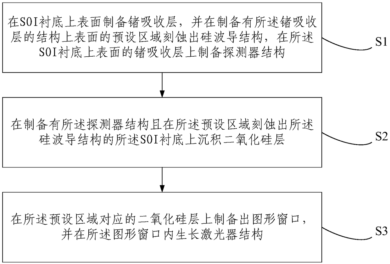
[0025] like figure 1 As shown, an embodiment of the present invention provides a method for preparing a monolithic silicon-based optoelectronic integrated chip, comprising:

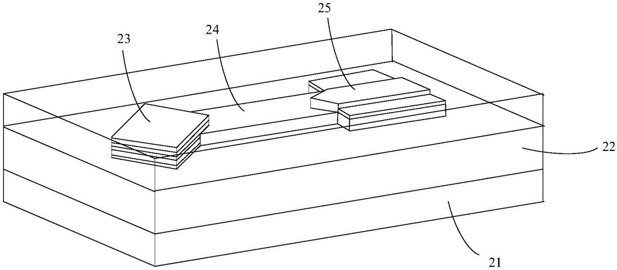
[0026] S1, preparing a germanium absorbing layer on the upper surface of the SOI substrate, and etching a silicon waveguide structure in a predetermined area on the upper su...


PUM


Abstract

The embodiment of the invention provides a preparation method of a monolithic silicon-based photoelectric integrated chip. A laser device structure grows by etching a pattern window on an SOI substrate, a detector structure grows on a silicon waveguide layer in the SOI substrate, and a laser device and a detector are connected through the etched silicon waveguide structure, so that integration ofthe on-chip laser device, the detector and the silicon waveguide structure is achieved. According to the preparation method of the monolithic silicon-based photoelectric integrated chip, the laser device structure grows by directly etching the pattern window, high repeatability and reliability are achieved, large-scale preparation can be achieved, the cost is greatly reduced, good application prospects are achieved, the blank that a practical on-chip photoelectric integration cannot be achieved through a direct selective area epitaxy mode at present is made up for, and the method particularlysolves the on-chip integration problem of the laser device and other devices.

Description

technical field [0001] Embodiments of the present invention relate to the technical field of silicon-based monolithic optoelectronic integration, and more specifically, to a method for preparing a monolithic silicon-based optoelectronic integrated chip. Background technique [0002] Today, the advancement of information technology is constantly promoting the development of society, and computer systems based on silicon-based microelectronic devices are penetrating into every aspect of people's lives. While enjoying the convenience brought by the advancement of information technology, people are also creating a large amount of data. With the explosive growth of data volume, how to quickly transmit and process these data has become a new challenge, especially in data center supercomputers and other application scenarios that require ultra-large-scale and ultra-high-speed data transmission and processing capabilities. [0003] The current microelectronic chip connects the vari...

Claims


Application Information

Patent Timeline
IPC IPC(8): G02B6/136
CPCG02B6/136
Inventor 王俊成卓杨泽园尹海鹰张翼东杨明黄永清任晓敏
Owner BEIJING UNIV OF POSTS & TELECOMM
Why Eureka
Try Eureka