On-chip integrated autocorrelator based on semiconductor nanowire

A nanowire and semiconductor technology, applied in the directions of light guides, instruments, nonlinear optics, etc., can solve the problems of difficult to achieve high-integration chip autocorrelation test, poor time resolution, etc., and achieve simple structure, high repeatability and reliability. , the effect of stable performance

Active Publication Date: 2020-09-18
ZHEJIANG UNIV
View PDF2 Cites 0 Cited by
  • Summary
  • Abstract
  • Description
  • Claims
  • Application Information

AI Technical Summary

Problems solved by technology

[0003] At present, the method that can realize pulse autocorrelation measurement on an integrated chip is mainly to use the two-photon absorption of silicon detectors, combined with the slow light effect of photonic crystals to realize the measurement of pulse width. This method requires a row of detector arrays with high time resolution. Poor, difficult to achieve highly integrated on-chip autocorrelation test

Method used


Image

  • On-chip integrated autocorrelator based on semiconductor nanowire

Examples


Embodiment Construction

[0026] The present invention will be further described below in conjunction with accompanying drawings and examples, but the protection scope of the present invention should not be limited thereby.

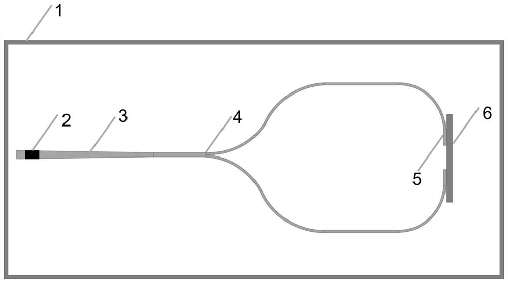
[0027] Such as figure 1 As shown, a grating 2, a transmission waveguide 3, a Y branch beam splitter 4, a coupling waveguide 5 and a semiconductor nanowire 6 are arranged on the substrate 1; the output end of the grating 2 is connected to the Y branch beam splitter 4 through the transmission waveguide 3 Collecting the input end, the two beam splitting output ends of the Y branch beam splitter 4 are respectively connected to the semiconductor nanowire 6 with the respective coupling waveguides 5, so that the Y branch beam splitter 4, the two coupling waveguides 5 and the semiconductor nanowire 6 are surrounded by into a drop-like shape. The Y-branch beam splitter 4 adopts a 50:50 1×2 beam splitter.

[0028] The specific implementation is along the propagation direction of the input...


PUM


Abstract

The invention discloses an on-chip integrated autocorrelator based on a semiconductor nanowire. A grating, a transmission waveguide, a Y-branch beam splitter, coupling waveguides and a semiconductor nanowire are arranged on a substrate. The output end of the grating is connected to the integrated input end of the Y-branch beam splitter through the transmission waveguide, and the two beam splittingoutput ends of the Y-branch beam splitter are connected to the two ends of the semiconductor nanowire through the respective coupling waveguides. Signal pulse light is coupled into the transmission waveguide from the grating on the substrate, is split by the Y-branch beam splitter and then is coupled into the semiconductor nanowire from the two ends of the semiconductor nanowire along the coupling waveguides on the two sides at the same time to generate transverse second harmonics. According to the invention, through optical coupling of the on-chip integrated waveguide etched by an electron beam and the semiconductor nanowire, measurement of the on-chip pulse width is realized, the repeatability and the reliability are high, and compared with a traditional autocorrelator, the on-chip integrated autocorrelator has the characteristics of miniaturization, easy integration and the like.

Description

technical field [0001] The invention relates to the technical fields of designing micro-optical elements, optical communication, and silicon-based monolithic optoelectronic integration, and more specifically relates to an integrated autocorrelator based on on-chip integrated waveguides and semiconductor nanowires. Background technique [0002] Ultrashort optical pulses are widely used in optical communication, nonlinear optical fiber, optical sensing and other fields. The rise of integrated optics makes ultrashort pulses also play an important role in integrated chips. The measurement and analysis of short pulses, and its small size, low cost, easy to use, and maintenance-free advantages can greatly expand its applications in optical communications, nonlinear optical fibers, and optical sensing. A key technique is optical autocorrelation measurement, which uses the pulse itself to measure its pulse width. [0003] At present, the method that can realize pulse autocorrelatio...

Claims


Application Information

Patent Timeline
IPC IPC(8): G01J11/00G02F1/377G02B6/12G02B6/136
CPCG01J11/00G02B6/12004G02B6/136G02F1/377
Inventor 童利民李维嘉郭欣鲍庆洋张建彬
Owner ZHEJIANG UNIV
Why Eureka
Try Eureka