Semiconductor device and preparation method thereof

A manufacturing method and semiconductor technology, applied in the direction of semiconductor devices, semiconductor/solid-state device manufacturing, electrical components, etc., can solve the problems of high source-drain contact resistance, etc., and achieve the effects of small contact resistance, reduced contact resistance, and good alignment

Pending Publication Date: 2019-03-15
INST OF MICROELECTRONICS CHINESE ACAD OF SCI
View PDF8 Cites 0 Cited by
  • Summary
  • Abstract
  • Description
  • Claims
  • Application Information

AI Technical Summary

Problems solved by technology

[0004] The main purpose of this application is to provide a semiconductor device and its manufacturing method to solve the problem of relatively large source-drain contact resistance of germanium-based devices in the prior art

Method used


Image

  • Semiconductor device and preparation method thereof
  • Semiconductor device and preparation method thereof
  • Semiconductor device and preparation method thereof

Examples


Embodiment

[0059] The fabrication process of semiconductor devices includes:

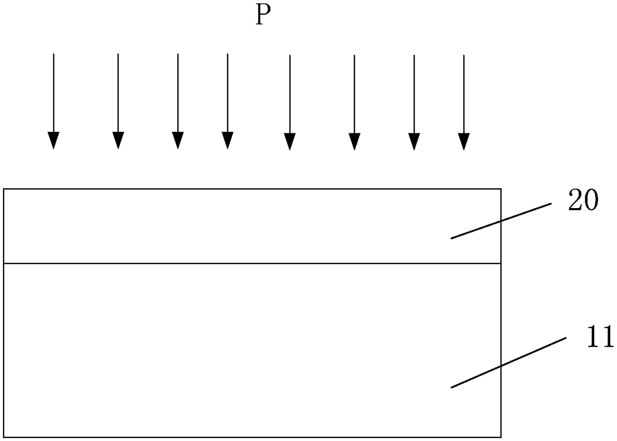
[0060] A germanium-based semiconductor preparation 10 is provided, the semiconductor preparation 10 includes a germanium substrate and a source region 11 and a drain region 12 arranged in the germanium substrate, figure 1 Only the source region 11 is shown in the figure, and the drain region 12 is the same as the source region 11, both of which are doped with N-type impurity P;

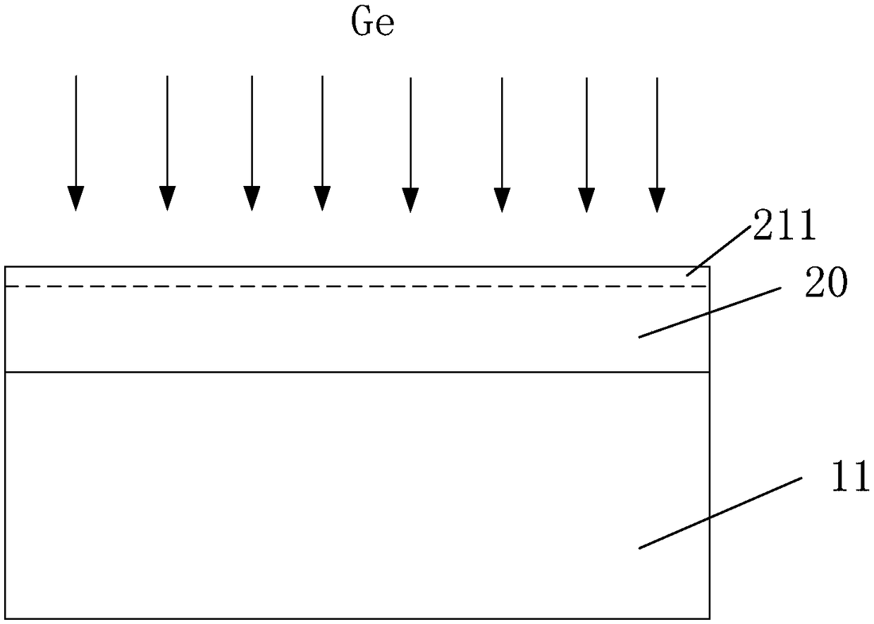
[0061] Pre-epitaxial layers 20 are respectively arranged on the exposed surfaces of the source region 11 and the drain region 12, and each of the above-mentioned pre-epitaxial layers 20 includes a base material and a second N-type impurity doped in the base material, and the base material is Silicon, the second N-type impurity is P, and the doping concentration of the above-mentioned second N-type impurity is 1.0×10 20 cm -3 ~9.0×10 21 cm -3 between, figure 2 It just shows that a pre-epitaxial layer 20 is provided on the surfac...


PUM


Abstract

The invention provides a semiconductor device and a preparation method thereof. The preparation method comprises the steps of providing a germanium-based semiconductor preparation body provided with asource region and / or a drain region, wherein doped impurities of the source region and / or the drain region are first N-type impurities; arranging a pre-epitaxial layer on an exposed surface of the source region and / or the drain region, wherein the pre-epitaxial layer comprises a base material and second N-type impurities doped in the base material; the base material comprises non-Ge IV group elements; and the doping concentration of the second N-type impurities is 1.0*10<20>cm<-3>-9.0*10<21>cm<-3>; injecting third impurities into the pre-epitaxial layer, so that the pre-epitaxial layer far away from the semiconductor preparation body is non-crystallized to form an epitaxial layer; arranging an electrode layer on the surface, far away from the source region and / or the drain region, of theepitaxial layer; and performing heat treatment on the semiconductor preparation body provided with the electrode layer to form source contact and / or drain contact. The contact resistance of the sourcecontact and / or the drain contact formed by the preparation method is low.

Description

technical field [0001] The present application relates to the field of semiconductors, and in particular, to a semiconductor device and a manufacturing method thereof. Background technique [0002] Due to its high and symmetrical carrier mobility, germanium material has become one of the promising development directions of high-performance MOS devices. However, there are still many problems to be solved in germanium-based NMOS devices, such as excessive source-drain contact resistance due to low activation concentration of N-type impurities, which limits the improvement of device performance. [0003] The above information disclosed in the Background section is only to enhance the understanding of the background of the technology described herein, therefore, the Background may contain certain information which is not formed in the country for those skilled in the art. known prior art. Contents of the invention [0004] The main purpose of the present application is to pr...

Claims


Application Information

Patent Timeline
IPC IPC(8): H01L29/06H01L29/16H01L21/336H01L29/78
CPCH01L29/0688H01L29/16H01L29/66409H01L29/78Y02P70/50
Inventor 罗军毛淑娟许静
Owner INST OF MICROELECTRONICS CHINESE ACAD OF SCI
Why Eureka
Try Eureka