
Silicon carbide Schottky diode

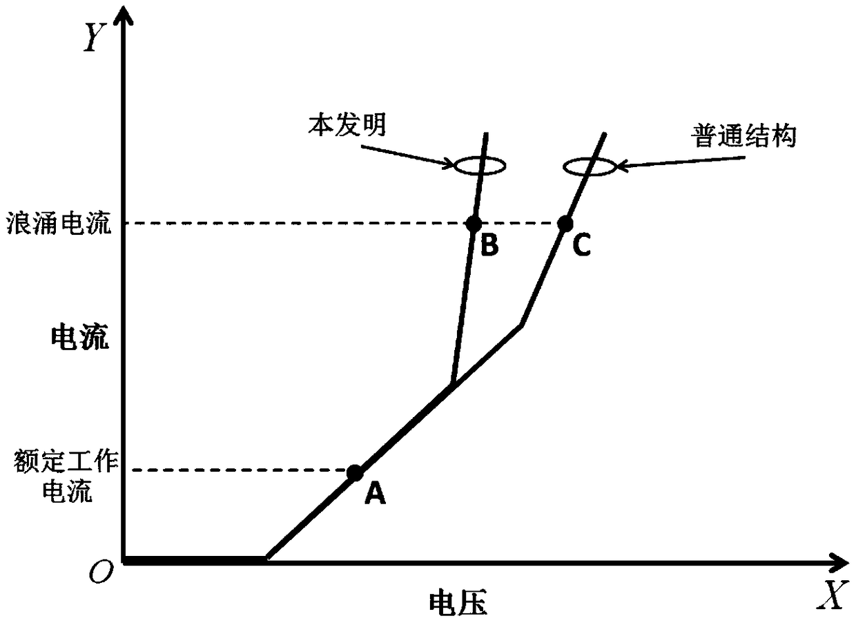
A technology of Schottky diode and silicon carbide, which is applied in the direction of electrical components, circuits, semiconductor devices, etc., can solve the problem of low anti-surge ability, achieve the effect of improving anti-surge ability and improving reliability

Pending Publication Date: 2019-03-15
北京国联万众半导体科技有限公司
View PDF6 Cites 1 Cited by
  • Summary
  • Abstract
  • Description
  • Claims
  • Application Information

AI Technical Summary

Problems solved by technology

[0005] An embodiment of the present invention provides a silicon carbide Schottky diode, aiming to solve the problem of low anti-surge capability of SiC Schottky diodes in the prior art

Method used


Image

  • Silicon carbide Schottky diode
  • Silicon carbide Schottky diode

Examples


Embodiment Construction

[0022] In order to enable those skilled in the art to better understand this solution, the technical solution in this solution embodiment will be clearly described below in conjunction with the accompanying drawings in this solution embodiment. Obviously, the described embodiment is a part of this solution Examples, but not all examples. Based on the embodiments in this solution, all other embodiments obtained by persons of ordinary skill in the art without creative efforts shall fall within the protection scope of this solution.

[0023] The term "comprising" and any other variants in the description and claims of this solution and the above drawings mean "including but not limited to", and are intended to cover non-exclusive inclusion.

[0024] The realization of the present invention is described in detail below in conjunction with specific accompanying drawing:

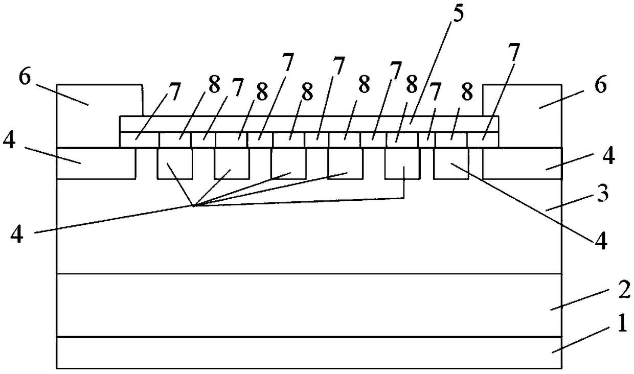
[0025] figure 1 A silicon carbide Schottky diode provided by an embodiment of the present invention is shown....


PUM

PropertyMeasurementUnit
Thicknessaaaaaaaaaa
Doping concentrationaaaaaaaaaa
Thicknessaaaaaaaaaa

Abstract

The invention discloses a silicon carbide Schottky diode, which comprises a cathode metal layer, an N+type substrate, an N-type epitaxial layer, P-type regions, a compound metal layer, a metal thickening layer and passivation layers, wherein the N+type substrate is arranged on the cathode metal layer; the N-type epitaxial layer is arranged on the N+type substrate; the P-type regions are arranged in the N-type epitaxial layer and are in a flush type with the upper surface of the N-type epitaxial layer; the compound metal layer is arranged on the N-type epitaxial layer; the metal thickening layer is arranged on the compound metal layer; the passivation layers are arranged on two ends of the N-type epitaxial layer and cover the periphery of the metal thickening layer; the P-type regions are arranged at intervals; and the compound metal layer comprises high potential energy barrier metal regions arranged in the P-type region, and low potential energy barrier metal regions arranged in the intervals of the high potential energy barrier metal regions. By use of the silicon carbide Schottky diode, the P-type regions and the high potential energy barrier metal regions are in contact, the N-type epitaxial layer and the low potential energy barrier metal regions are in contact, the P-type regions and the N-type epitaxial layer adopt different contact metals, and the anti-surge capabilityof the silicon carbide Schottky diode is improved.

Description

technical field [0001] The invention relates to the technical field of semiconductor devices, in particular to a silicon carbide Schottky diode. Background technique [0002] Silicon carbide (SiC) Schottky diodes are multi-carrier conduction devices. Unlike silicon PiN diodes, which have a conductance modulation effect when they are forward-conducting, there is no unbalanced minority carrier in the drift region of SiC Schottky diodes to participate in conduction. Therefore, the reverse recovery speed of SiC Schottky diodes is fast, and the reverse recovery charge is extremely small, which is about 10% of that of silicon PiN diodes of the same level. Correspondingly, when SiC Schottky diodes are used in circuits The resulting loss is also reduced to less than 10%. [0003] For diodes, the forward surge current value is an important indicator to consider device performance. In the actual circuit, due to occasional reasons such as external signal interference and grid voltage...

Claims


Application Information

Patent Timeline
IPC IPC(8): H01L29/872H01L29/16H01L29/06
CPCH01L29/0684H01L29/1608H01L29/872
Inventor 张力江王永维付兴中周国樊帆杨志虎马杰王国清李飞廖龙忠毕胜赢梁东升崔玉兴
Owner 北京国联万众半导体科技有限公司
Learn More