Supercharge Your Innovation With Domain-Expert AI Agents!

Array substrate and preparation method thereof, display panel, and display device

An array substrate and array technology, applied in semiconductor/solid-state device manufacturing, electrical components, electrical solid-state devices, etc., can solve the problems of scratching the alignment film in the display area, easy sliding, and light leakage in the display area, and improve product yield. and stability, the effect of large cost advantage

Active Publication Date: 2019-03-22
BOE TECH GRP CO LTD +1
View PDF4 Cites 1 Cited by
  • Summary
  • Abstract
  • Description
  • Claims
  • Application Information

AI Technical Summary

Problems solved by technology

However, its disadvantage is that the coating of the organic film has a high step coverage, and its upper surface is relatively flat and smooth, so that the surface of the final array substrate is relatively smooth. PS) The top is not fixed, PS is easy to slide on the surface of the array substrate, scratching the alignment film of the display area, resulting in light leakage in the display area

Method used


Image

  • Array substrate and preparation method thereof, display panel, and display device
  • Array substrate and preparation method thereof, display panel, and display device
  • Array substrate and preparation method thereof, display panel, and display device

Examples


Embodiment Construction

[0031] The following will clearly and completely describe the technical solutions in the embodiments of the present invention with reference to the accompanying drawings in the embodiments of the present invention. Obviously, the described embodiments are only some, not all, embodiments of the present invention. Based on the embodiments of the present invention, all other embodiments obtained by persons of ordinary skill in the art without making creative efforts belong to the protection scope of the present invention.

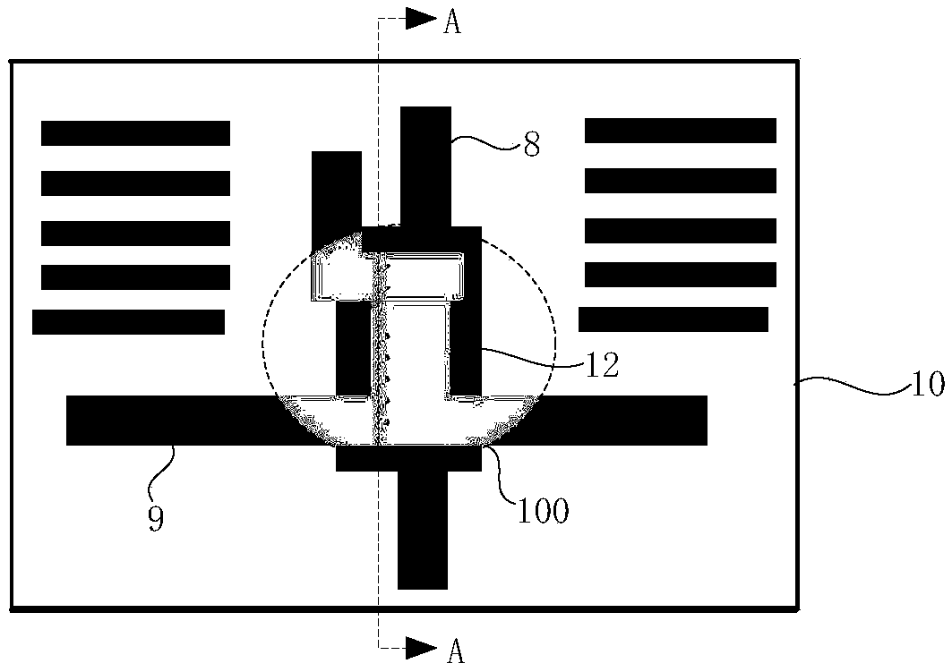
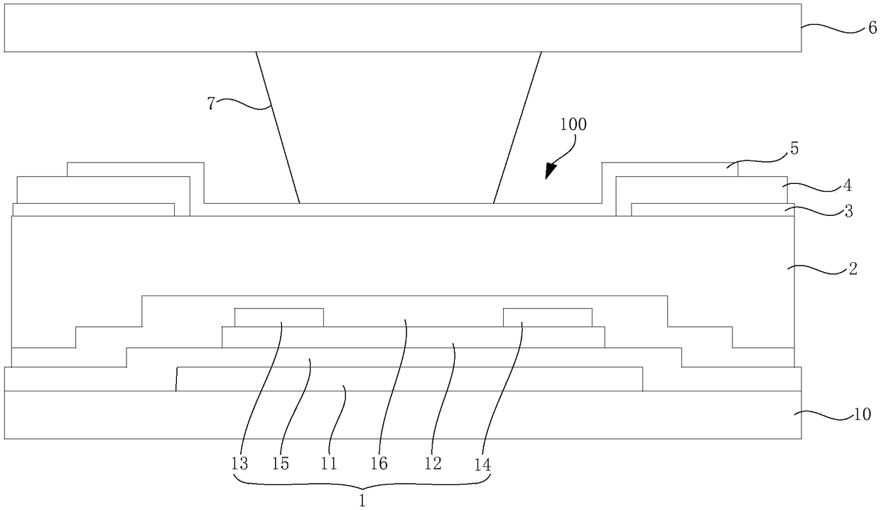
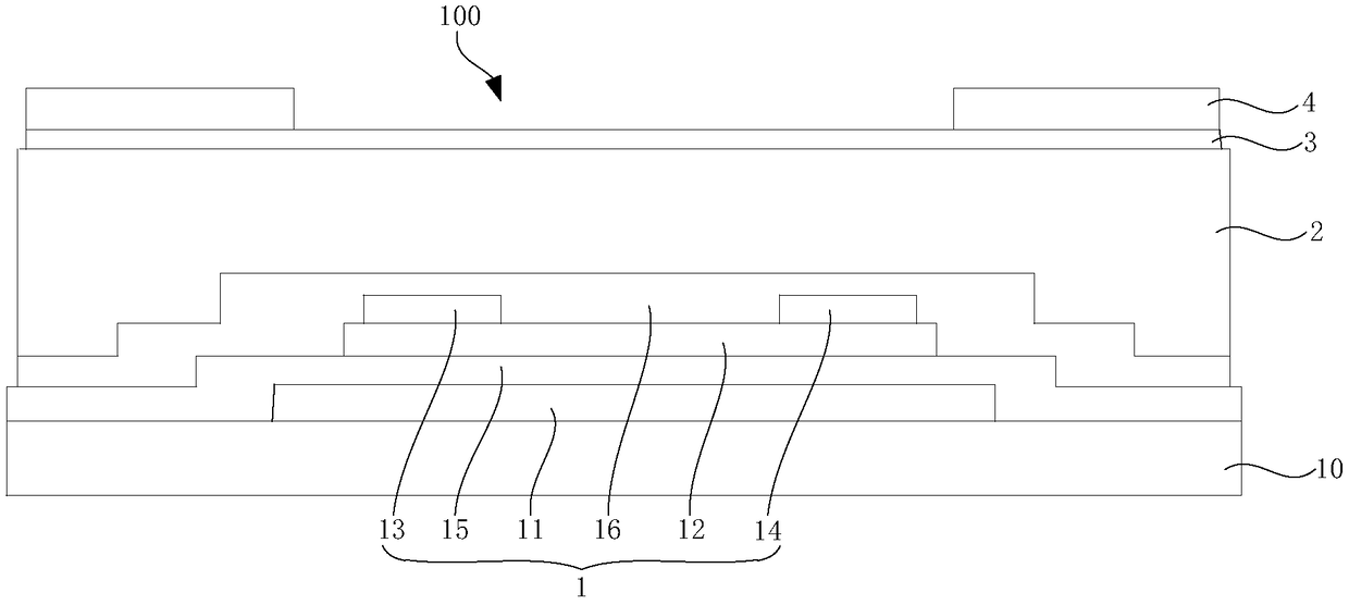
[0032] like Figure 1-Figure 5 As shown, the embodiment of the present invention provides an array substrate, including an array of thin film transistors 1, and an organic insulating layer 2, a first electrode layer 3, and a first insulating layer 4 sequentially stacked on the thin film transistor 1, wherein:

[0033] At least one of the organic insulating layer 2, the first electrode layer 3, and the first insulating layer 4 is provided with a slot correspond...


PUM


Abstract

The invention, which relates to the technical field of display, discloses an array substrate and a preparation method thereof, a display panel, and a display device. The array substrate comprises thin-film transistors distributed in an array, an organic insulating layer, a first electrode layer, and a first insulating layer, wherein the organic insulating layer, the first electrode layer, and thefirst insulating layer are laminated on the thin-film transistors. At least one of the organic insulating layer, the first electrode layer, and the first insulating layer is provided with a slot holecorresponding to an insulation mat, so that a recessed part is formed at the position, corresponding to the insulation mat, of the surface of the array substrate. Since the recessed part is formed onthe surface of the array substrate, the top of the insulation mat can be inserted into the recessed part when alignment is carried out to realize limiting and preventing sliding, so that scratching ofthe alignment film of the display zone by the insulation mat is avoided and thus the yield and stability are improved. Moreover, compared with the array substrate preparation process in the prior art, no process is added during the reparation process of the array substrate; and the preparation process does not change, so that the cost is lowered.

Description

technical field [0001] The present invention relates to the field of display technology, in particular to an array substrate and a preparation method thereof, a display panel, and a display device. Background technique [0002] At present, high-resolution array substrate products generally use an organic insulating film to cover the thin-film transistor array. After coating, exposure, development, and curing, the stress of the organic insulating film is very low, but the thickness can reach more than 3.0um, which can effectively reduce capacitance. , to meet the requirements of high resolution and low power consumption products. However, its disadvantage is that the coating of the organic film has high step coverage, and its upper surface is relatively flat and smooth, so that the surface of the final array substrate is relatively smooth. The top of the PS) is not fixed, and the PS is easy to slide on the surface of the array substrate, scratching the alignment film of the ...

Claims


Application Information

Patent Timeline
Patent Type & Authority Applications(China)
IPC IPC(8): H01L27/12H01L21/77
CPCH01L27/124H01L27/1248H01L27/1259
Inventor 田茂坤黄中浩谌伟郭瑞花
Owner BOE TECH GRP CO LTD
Features
  • R&D
  • Intellectual Property
  • Life Sciences
  • Materials
  • Tech Scout
  • Unparalleled Data Quality
  • Higher Quality Content
  • 60% Fewer Hallucinations
Learn More