Reliability evaluation multilayer circuit board

A multi-layer circuit and reliability technology, applied in the direction of printed circuit, printed circuit, printed circuit manufacturing, etc., can solve the problems of inability to test and judge product reliability, affect product performance, and lack of uniformity, and achieve low manufacturing cost, Capacity mastery, obvious effect

Pending Publication Date: 2019-03-22
DALIAN CHONGDA CIRCUIT
0 Cites 0 Cited by

AI-Extracted Technical Summary

Problems solved by technology

At present, the reliability testing process of circuit board products is very complicated, and the process methods are also in different styles, but there is no unified standard. The test is carried out by technicians according to their own experience, level, professional knowledge, etc. Due to different methods...

Method used

Because each hole wall state test area all needs to do slice grinding process, in order to improve processing speed, can increase the processing location hole of hole wall state test hole and slice make the design of location hole in hole wall state test area, use The pins connect multiple circuit boards together for grinding, which can improve the grinding efficiency. Hole wall state test hole processing positioning hole and slice production positioning hole can be processed by drilling process.
In summary, the present invention is by combining a plurality of important reliability tests in the circuit board processing technology on a reliability test circuit board and completes through a processing technology, can scientifically and accurately do product reliability performance It can make accurate judgment and identification, and has the characteristics of simple operation, reasonable design, capacity control, low manufacturing cost and obvious effect.
[0028] The conductive test circuit is used for the circuit connectivity test. The multilayer circuit board in the dril...

Abstract

The invention discloses a reliability evaluation multilayer circuit board. The reliability evaluation multilayer circuit board comprises a plurality of test regions; each test region comprises a drilled area and a hole wall state test area; the test holes of the drilled areas of the different test regions have different apertures; each drilled area includes a test hole array of the same aperture machined by the same drill bit; the inner wall of the test hole is provided with a conductive layer and a protective layer distributed sequentially from inside to outside; test lines which are arrangedbetween different layers of the multilayer circuit board and at the outer layers of the multilayer circuit board and are located between the test holes are connected in series so as to form a conductive test line; the outer circuit board of the drilled area is further provided with two connectivity test pads which are connected to the test holes corresponding to the start end and tail end of theconductive test line through a wire; and each hole wall state test area includes hole wall state test holes which are machined in the hole wall state test area by the same bit for machining the test holes after a certain number of test holes from the first test hole which are machined by the bit. With the reliability evaluation multilayer circuit board of the invention adopted, the reliability ofproducts can be judged scientifically and accurately.

Application Domain

Printed circuit aspectsInspection/indentification of circuits +2

Technology Topic

Drill bitElectrical and Electronics engineering +1

Image

  • Reliability evaluation multilayer circuit board
  • Reliability evaluation multilayer circuit board
  • Reliability evaluation multilayer circuit board

Examples

  • Experimental program(1)

Example Embodiment

[0021] The specific embodiments of the present invention will be further described in detail below with reference to the accompanying drawings.
[0022] It should be noted that in the following specific embodiments, when the embodiments of the present invention are described in detail, in order to clearly show the structure of the present invention for ease of description, the structure in the drawings is not drawn according to the general scale. Partial enlargement, deformation, and simplification of processing have been implemented. Therefore, this should be avoided as a limitation of the present invention.
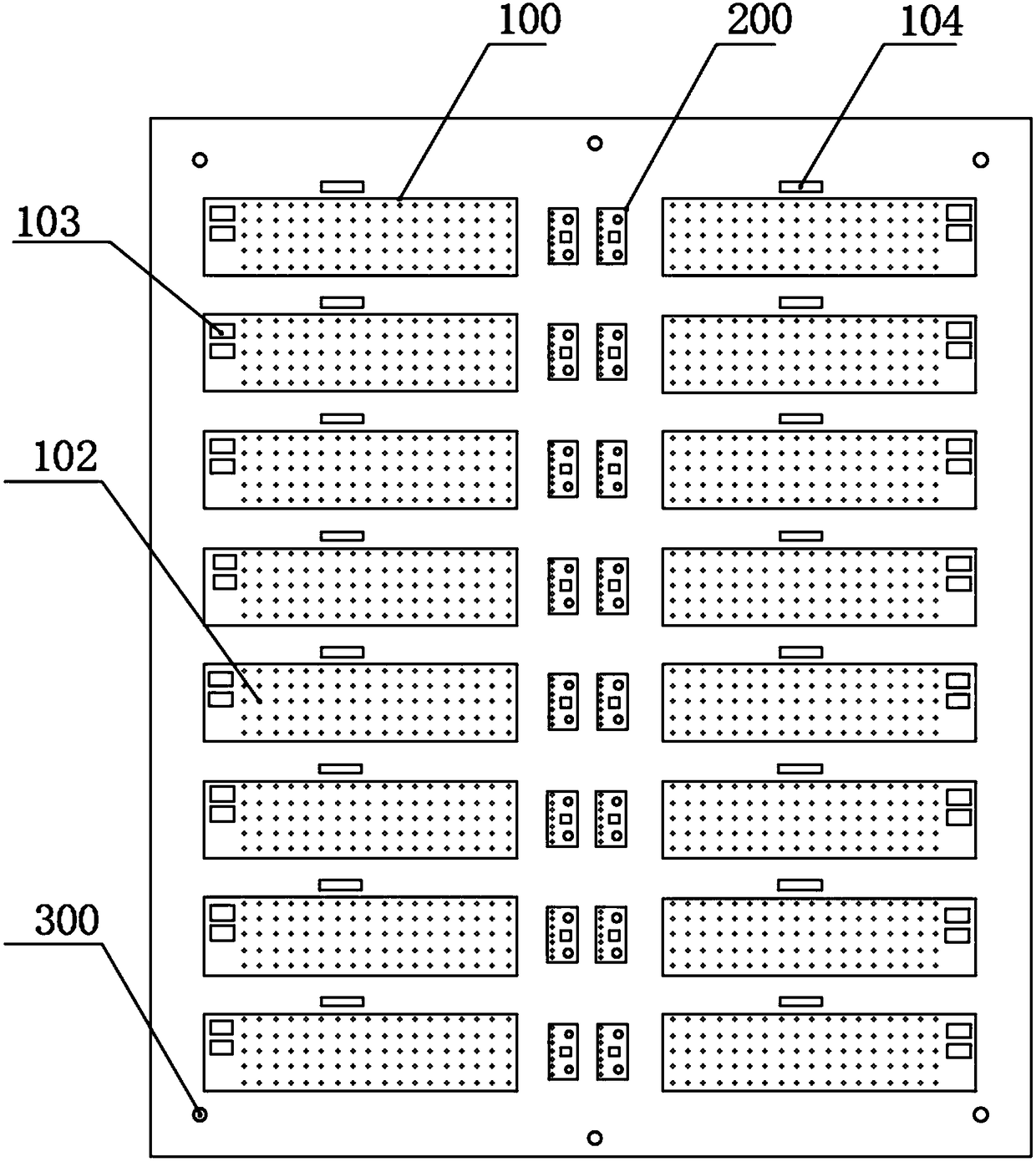
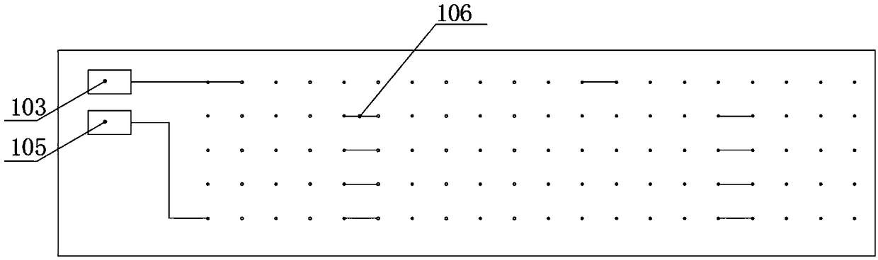
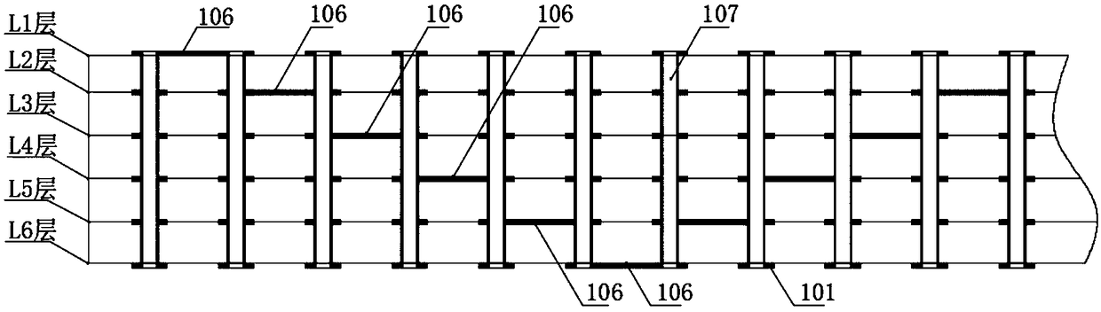
[0023] The more important reliability evaluation includes the material test of the circuit board base material, the circuit reliability and mechanical performance reliability of the processed circuit board under extreme environments, and the circuit board base material and circuit board processing parameters match each other. The reliability of the finished circuit board is higher. The invention evaluates the reliability of the finished circuit board made of a specific batch of circuit board substrates using a specific circuit board processing technology.
[0024] In the following specific embodiments of the present invention, please refer to Figure 1 ~ Figure 4. As shown in the figure, a reliability evaluation multilayer circuit board includes a plurality of test areas, each test area includes a drilled area and a hole wall state test area, and the hole diameters of the drilled areas in different test areas are different. The diameter of the test hole in each test area is summarized from the circuit board processing technology.
[0025] Each drilling area includes an array of test holes with the same aperture processed by the same drill bit, starting from the first hole of the test hole array, and for every certain number of test holes processed, a hole wall state test hole is processed in the hole wall state test area . Since the same drill bit is used, the hardness of the circuit board substrate can be indirectly judged by the wear of the drill bit. The test hole array pattern is based on the principle of as many test holes as possible, usually several thousand to tens of thousands.
[0026] The inner wall of the test hole has a conductive layer and a protective layer in turn from the inside to the outside. The test circuit between the test hole and the test hole located between the layers of the multilayer circuit board and the outer layer constitutes a conductive test circuit; the outer layer of the drilled area The circuit board also has two continuity test pads, which are respectively connected to test holes corresponding to the start and end of the conductive test circuit through a wire.
[0027] In this embodiment, the specific implementation of the conductive test circuit refers to figure 2 with image 3 , The conductive test circuit is composed of multiple test circuits in series. The test circuits are evenly distributed in the interlayer and outer layer of the circuit board in the entire drilling area, and the cross-sectional direction along the thickness of the multilayer circuit board in each row of test holes is " V"-shaped polyline distribution. Specifically, taking a 6-layer circuit board as an example, including the L1 to L6 layers, the test circuit is etched on each surface, and the first connectivity test pad 103 is established on the L1 layer of the multilayer circuit board. The continuity test pad 103 is connected to the first hole in the first row of the L1 layer of the laminated circuit board with a wire, and the first hole in the first row of the L1 layer of the laminated circuit board is connected to the length of the test area The second hole of the L2 layer is connected with a test line, and the second hole of the L2 layer of the laminated circuit board is connected with the third hole along the length of the test area with a test line, and then connected to the sixth layer of the L6 layer circuit board. The hole and the seventh hole are connected by a test circuit, and then connected upward in the thickness direction, that is, the seventh hole and the eighth hole of the fifth layer of the laminated circuit board are connected by a test circuit until the test holes in the first row are all connected. Adopt the principle of proximity, connect to the second row of test holes, and then continue to arrange the test lines between the second row of test holes in the same way as the test lines of the first row of test holes between layers in the direction from right to left. Until all the test holes in all rows are connected to the test circuit, the last test hole is connected to the second continuity test pad 105 through a wire. Preferably, the periphery of the test hole is connected to the test circuit through a pad.
[0028] The conductive test circuit is used for circuit continuity testing. The multi-layer circuit board in the drilled area is subjected to a thermal stress test, soaked in a tin-lead pot at 188°C for about 10 seconds, and repeated 3-6 times. Use a resistance tester to test the change rate of the resistance between the two continuity test pads before and after the thermal stress experiment, and evaluate the reliability of the circuit board interlayer and outer circuit according to the resistance change rate. Generally, no more than 2% is considered qualified, or the evaluation is based on industry standards or customer requirements. If the resistance value changes too much, the conductive circuit is disconnected in the destructive experiment. Use a resistance tester to connect any test hole to determine the specific location of the conductive circuit (for example, which layer of circuit board). Due to the large number of test holes, the specific locations where the disconnection occurs are counted, and the statistical results are more reliable, and the process steps represented by the locations where more disconnections occur are the process steps that need improvement.
[0029] Each hole wall state test area includes the same drill bit that processes the test hole. Starting from processing the first test hole, the hole wall state test hole is processed in the hole wall state test area after a certain number of test holes are spaced. Use the multi-layer circuit board in the hole wall state test area to test the impact resistance, abrasion resistance, tear resistance of the circuit board and the bonding strength between different materials. The multi-layer circuit board in the hole wall state test area is subjected to the thermal stress test, and Soak them in a tin-lead pot at 188°C for about 10 seconds, and repeat 3-6 times. Then, the hole wall state test hole is ground half of the hole, and the impact resistance and wear resistance of the circuit board are evaluated by comparing the changes in the hole wall roughness state of the sequentially processed hole wall state test hole. By observing the copper layer and the copper protective layer The bonding state evaluates the bonding strength between the materials, and the tear resistance of the circuit board is evaluated by observing the wick effect between the copper layer and the substrate.
[0030] Since all the holes on this slice are processed by the tool at an interval of 499 holes, it is basically possible to evaluate the state of the hole wall of this type of material under different tool diameters, different tool wear conditions, and different ambient temperatures, and have a certain coverage , Can accurately and scientifically judge the stability of the material's physical properties and chemical properties.
[0031] Since each hole wall state test area needs to be sliced ​​and polished, in order to increase the processing speed, the hole wall state test hole processing positioning hole and the design of slicing to make the positioning hole can be added to the hole wall state test area. Two circuit boards are connected together for grinding, which can improve the grinding efficiency. Hole wall state test hole processing positioning holes and slices to make positioning holes can be processed by drilling technology.
[0032] In order to avoid confusion, a logo design can be added to each drilling area and hole wall state test area, and the logo can be processed by drilling technology.
[0033] The edge of the multilayer circuit board also includes process positioning holes, which is convenient for positioning and use in the circuit board processing technology.
[0034] The method for preparing the reliability evaluation multilayer circuit board includes the following steps:
[0035] Step S1: Design the multilayer circuit board according to the above reliability evaluation, including determining the number of layers of the multilayer circuit board, the number of test areas, the number of rows and columns of the test hole array, the number of test holes, and the number of test holes. The distance between the holes, the position and number of the hole wall state test holes, the inner and outer patterns of the multilayer circuit board, etc.
[0036] Step S2: Perform reliability evaluation of the production of multilayer circuit boards, according to preliminary preparation → engineering design → cutting → blanking → selling → inner layer production → lamination → drilling → electroless plating → electroplating → outer layer pattern production Reliability evaluation multi-layer circuit board is obtained by process steps.
[0037] Step S3: Cut the circuit boards in each drilling area and hole wall state test area, and perform circuit connectivity tests and circuit board impact resistance, abrasion resistance, tear resistance, and bonding strength tests between different materials.
[0038] In summary, the present invention combines multiple important reliability tests in the circuit board processing technology on one reliability test circuit board and completes it through a single processing technology, which can scientifically and accurately make accurate judgments on product reliability. And identification, it has the characteristics of simple operation, reasonable design, capacity control, low manufacturing cost, and obvious effect.
[0039] The above are only preferred specific embodiments of the present invention, but the protection scope of the present invention is not limited to this. Anyone familiar with the technical field within the technical scope disclosed by the present invention, according to the technical solution of the present invention Equivalent replacements or changes to its inventive concept should all fall within the protection scope of the present invention.

PUM

no PUM

Description & Claims & Application Information

We can also present the details of the Description, Claims and Application information to help users get a comprehensive understanding of the technical details of the patent, such as background art, summary of invention, brief description of drawings, description of embodiments, and other original content. On the other hand, users can also determine the specific scope of protection of the technology through the list of claims; as well as understand the changes in the life cycle of the technology with the presentation of the patent timeline. Login to view more.

Similar technology patents

Laser radar optical system with optical axis calibrating function and optical axis calibrating method

InactiveCN102353950AOptical axis alignment with high precisioneasy to operate
Owner:INST OF APPLIED ELECTRONICS CHINA ACAD OF ENG PHYSICS +1

Defrosting control method and device

ActiveCN104807132Aeasy to operateDefrost is reasonable
Owner:GREE ELECTRIC APPLIANCES INC OF ZHUHAI

Judgment method and device for high-altitude object throwing

PendingCN114241012AAccurate identification and judgmentRealize accurate traceability and early warning
Owner:SHENZHEN YANCHAO TECH

Classification and recommendation of technical efficacy words

  • easy to operate
  • Accurate identification and judgment

Lancet device

InactiveUS7303573B2inexpensively mass-producedeasy to operate
Owner:ABBOTT DIABETES CARE INC

Rapid and non-invasive optical detection of internal bleeding

InactiveUS20050065436A1easy to operaterapid and accurate result
Owner:HO WINSTON ZONH +2

Judgment method and device for high-altitude object throwing

PendingCN114241012AAccurate identification and judgmentRealize accurate traceability and early warning
Owner:SHENZHEN YANCHAO TECH
Why Eureka
Try Eureka