Silicon wafer for calibration, preparation method thereof and application thereof

A technology of silicon wafers and negatives, which is applied in the field of silicon wafers, can solve the problems of not meeting the requirements of cost control, inaccurate measurement of the number of particles, and high price of master chips, so as to achieve good spraying effect, meet the needs of daily monitoring, and reduce costs. low effect

Active Publication Date: 2019-03-26
SHANGHAI ADVANCED SILICON TECH CO LTD +1
View PDF9 Cites 0 Cited by
  • Summary
  • Abstract
  • Description
  • Claims
  • Application Information

AI Technical Summary

Problems solved by technology

Therefore, the use of standard sheets is very frequent, and particle standard sheets are different from standard sheets with other mechanical parameters. The frequency of use will directly affect the size and number of particles on the surface of the standard sheet. Peak shifts are prone to occur during calibration, and the number of particles cannot be measured. standard situation
However, the master chip of granular standard chips is expensive, and frequent replacement of new standard chips does not meet the requirements of cost control.

Method used


Image

  • Silicon wafer for calibration, preparation method thereof and application thereof
  • Silicon wafer for calibration, preparation method thereof and application thereof
  • Silicon wafer for calibration, preparation method thereof and application thereof

Examples


Embodiment 1

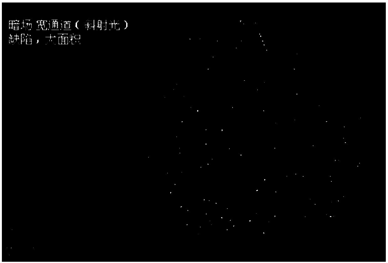
[0048] This embodiment provides a silicon chip for correction, the number of particles on the surface of the silicon chip for correction is 17021pcs, and the surface particle density is 60pcs / cm 2 .

[0049] Described preparation method comprises the steps:

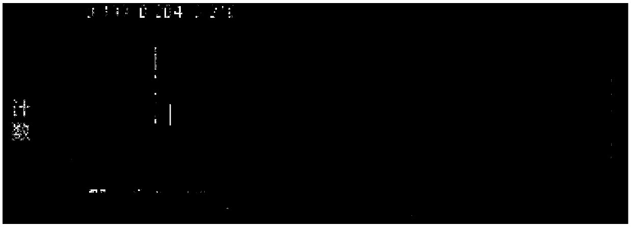
[0050] In a tenth-class clean room, the standard particle liquid with a particle size of 0.204 μm is sprayed vertically on the surface without scratches and the number of particles on the surface is less than 100 through the atomizer with an atomization rate of 0.2mL / min as a concentric path. On the 8-inch substrate, the spraying time is 16s, the distance between the atomizer nozzle and the substrate is 5cm, the concentric circle path starts from the center of the circle, and completes 4 concentric circles from the inside to the outside to obtain a silicon wafer for calibration.

[0051] In the tenth class clean room, the particle detector KAL Tencor SP1 is calibrated with a standard chip with a particle size of 0.204 μm...

Embodiment 2

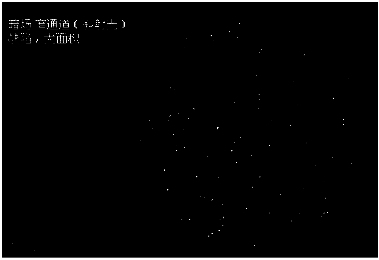
[0058] This embodiment provides a silicon chip for correction, the number of surface particles of the silicon chip for correction is 17359pcs, and the surface particle density is 100pcs / cm 2 .

[0059] Described preparation method comprises the steps:

[0060] In the tenth class clean room, the standard particle liquid with a particle size of 0.155 μm is sprayed vertically on the surface without scratches and the number of particles on the surface is less than 100 through the atomizer with an atomization rate of 0.2mL / min as a concentric path. On the 8-inch substrate, the spraying time is 16s, the distance between the atomizer nozzle and the substrate is 5cm, the concentric circle path starts from the center of the circle, and completes 4 concentric circles from the inside to the outside to obtain a silicon wafer for calibration.

[0061] In the tenth-class clean room, the particle detector KAL Tencor SP1 is calibrated with a standard chip with a particle size of 0.155 μm to ...

Embodiment 3

[0064] This embodiment provides a silicon chip for correction, the number of surface particles of the silicon chip for correction is 16556pcs, and the surface particle density is 30pcs / cm 2 .

[0065] Described preparation method comprises the steps:

[0066] In the tenth class clean room, the standard particle liquid with a particle size of 1.112 μm is sprayed vertically on the surface without scratches and the number of particles on the surface is less than 100 through an atomizer with an atomization rate of 0.2mL / min as a concentric path. On the 8-inch substrate, the spraying time is 16s, the distance between the atomizer nozzle and the substrate is 5cm, the concentric circle path starts from the center of the circle, and completes 4 concentric circles from the inside to the outside to obtain a silicon wafer for calibration.

[0067] In the tenth class clean room, the particle detector KAL Tencor SP1 is calibrated with a standard sheet with a particle size of 1.112 μm to o...


PUM


Abstract

The invention provides a silicon wafer for calibration, a preparation method thereof and application thereof. The silicon wafer for calibration has a surface particle number of 14000 to 20000pcs and asurface particle density of 30 to 100pcs/cm2. The preparation method is simple and low in price, and can be applied to industrial production. The prepared silicon wafer for calibration can meet the calibration accuracy of a particle detector, meets the needs for daily monitoring, reduces the frequency of use of a standard chip, and prolongs the service life of the standard chip so as to greatly reduce production cost.

Description

technical field [0001] The invention belongs to the field of silicon wafers, and relates to a calibration silicon wafer, its preparation method and application. Background technique [0002] Silicon wafer is the most important semiconductor material. At present, more than 90% of chips and sensors are manufactured based on semiconductor single crystal silicon wafer. The particles on the surface of silicon wafer will affect the electrical performance of integrated circuits. Too many particles on the surface will affect the subsequent The epitaxial processing and device formation will cause graphics defects, epitaxial defects, device failure, and affect the integrity of wiring, which will lead to product quality loss and low product yield. Therefore, it is necessary to strictly control the particle situation in the quality process of silicon wafers. [0003] The detection of particles on the surface of silicon wafers mainly relies on particle detection equipment. In order to e...

Claims


Application Information

Patent Timeline
Patent Type & Authority Applications(China)
IPC IPC(8): H01L21/66
CPCH01L22/12
Inventor 沈蓓颖沈思情徐伟张俊宝陈猛
Owner SHANGHAI ADVANCED SILICON TECH CO LTD
Why Eureka
Try Eureka