Color film substrate and manufacturing method thereof

A color filter substrate and mask technology, applied in instruments, nonlinear optics, optics, etc., can solve problems such as poor peripheral display, and achieve the effect of solving poor peripheral display, reducing production process steps, and improving economic benefits

Active Publication Date: 2019-04-02
NANJING CEC PANDA FPD TECH CO LTD
View PDF6 Cites 13 Cited by
  • Summary
  • Abstract
  • Description
  • Claims
  • Application Information

AI Technical Summary

Problems solved by technology

[0004] In order to solve the above problems, a color filter substrate and its manufacturing method are provided, which can ensure that the box thickness of the display area and the non-display area are consistent without increasing the box thickness of the display area, and solve the problem of poor peripheral display

Method used


Image

  • Color film substrate and manufacturing method thereof
  • Color film substrate and manufacturing method thereof
  • Color film substrate and manufacturing method thereof

Examples


Embodiment 1

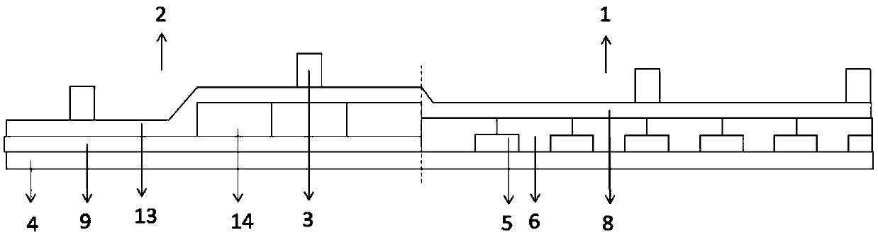
[0046] figure 2It is a structural schematic diagram of the first embodiment of the present invention, a color filter substrate, including: a display area 1 and a non-display area 2 located around the display area 1, the display area 1 includes a plurality of first black matrices 5 arranged in matrix, A plurality of pixel areas defined by the first black matrix 5, a color-resist layer 6 located in each pixel area, and a first planarization layer 8 covering the color-resist layer 6, the color-resist layer 6 partially covers the first black matrix5. The non-display area 2 includes a second black light-shielding layer 9 , a pad layer covering the second black light-shielding layer 9 , and a second planarization layer 13 covering the pad layer.

[0047] The color filter substrate further includes a plurality of support pillars 3 disposed on the first planarization layer 8 and the second planarization layer 13 .

[0048] In this embodiment, each pixel area is provided with three ...

Embodiment 2

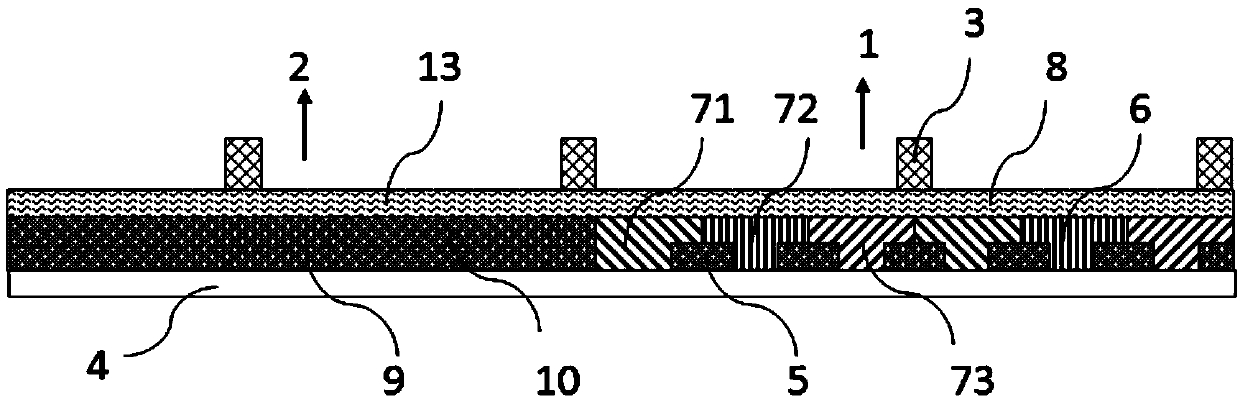
[0054] image 3 It is a structural schematic diagram of the second embodiment of the present invention, a color filter substrate, including: a display area 1 and a non-display area 2 located around the display area 1, the display area 1 includes a plurality of first black matrices 5 arranged in a matrix, A plurality of pixel areas defined by the first black matrix 5, a color-resist layer 6 located in each pixel area, and a first planarization layer 8 covering the color-resist layer 6, the color-resist layer 6 partially covers the first black matrix5. The non-display area 2 includes a second black light-shielding layer 9 , a pad layer covering the second black light-shielding layer 9 , and a second planarization layer 13 covering the pad layer.

[0055] The color filter substrate further includes a plurality of support pillars 3 disposed on the first planarization layer 8 and the second planarization layer 13 .

[0056] In this embodiment, each pixel area is provided with thr...

Embodiment 3

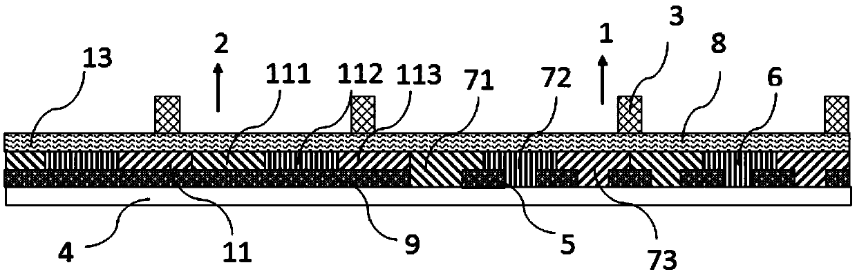
[0065] Figure 4 It is a structural schematic diagram of the third embodiment of the present invention, a color filter substrate, including: a display area 1 and a non-display area 2 located around the display area 1, and the display area 1 includes a plurality of first black matrices 5 arranged in a matrix, A plurality of pixel areas defined by the first black matrix 5, a color-resist layer 6 located in each pixel area, and a first planarization layer 8 covering the color-resist layer 6, the color-resist layer 6 partially covers the first black matrix5. The non-display area 2 includes a second black light-shielding layer 9 , a pad layer covering the second black light-shielding layer 9 , and a second planarization layer 13 covering the pad layer.

[0066] The color filter substrate further includes a plurality of support pillars 3 disposed on the first planarization layer 8 and the second planarization layer 13 .

[0067] The pad layer is the third planarization layer 12 , ...


PUM


Abstract

The invention discloses a color film substrate, and belongs to the field of the liquid crystal display. The color film substrate comprises a display area and a non-display area located surrounding thedisplay area; the display area comprises a first black matrix, pixel areas limited through the first block matrix, a color resistance layer located at each pixel area, and a first planarization layercovering the color resistance layer; the color resistance layer partially covers the first black matrix; the non-display area comprises a second black shading layer in whole surface laying, a cushionlayer covering the second black shading layer and a second planarization layer covering the cushion layer; the total height of the cushion layer and the second black shading layer is equal to the height of the color resistance layer. The color film substrate for flattening the display area and the non-display area can solve the problem that the periphery display is bad under the condition of notincreasing the thickness of the display area.

Description

technical field [0001] The invention relates to the technical field of liquid crystal display, in particular to a color filter substrate and a manufacturing method thereof. Background technique [0002] Liquid crystal display has the advantages of small size, low power consumption, and no radiation. It has developed rapidly in recent years and currently occupies a dominant position in the flat panel display market. The structure of the color filter substrate is generally as follows: figure 1 As shown, it includes a display area 1 and a non-display area 2. The display area 1 includes a first black matrix 5, a pixel area defined by the first black matrix 5, a color-resist layer 6 covering the pixel area, and a color-resist layer covering the color-resist layer. The first planarization layer 8, the non-display area 2 includes a second black light-shielding layer 9, an overlapping pixel color-resist layer 14 near the edge of the display area 1, and partially covering the second...

Claims


Application Information

Patent Timeline
Patent Type & Authority Applications(China)
IPC IPC(8): G02F1/1335G02F1/1333
CPCG02F1/1333G02F1/133512G02F1/133514G02F1/133516G02F1/133357
Inventor 李世春金潘祝宏勋许家诚王志军
Owner NANJING CEC PANDA FPD TECH CO LTD
Why Eureka
Try Eureka