Circuits and methods providing electronic band gap (EBG) structures at memory module electrical coupling

A memory module, electronic bandgap technology, applied in circuits, printed circuits, circuit devices, etc., can solve problems such as performance degradation, affecting bit capture, blocking, etc.

Active Publication Date: 2019-04-02
QUALCOMM INC
View PDF10 Cites 2 Cited by
  • Summary
  • Abstract
  • Description
  • Claims
  • Application Information

AI Technical Summary

Problems solved by technology

In a daisy-chain architecture, each of the memory modules is connected to a common bus, and electromagnetic reflections can affect the capture of bits at memory modules closer to the processor
Therefore, the severity of electromagnetic reflection phenomena seen at closer memory modules can set limits on the maximum bit rate between pr

Method used


Image

  • Circuits and methods providing electronic band gap (EBG) structures at memory module electrical coupling
  • Circuits and methods providing electronic band gap (EBG) structures at memory module electrical coupling
  • Circuits and methods providing electronic band gap (EBG) structures at memory module electrical coupling

Examples


Embodiment Construction

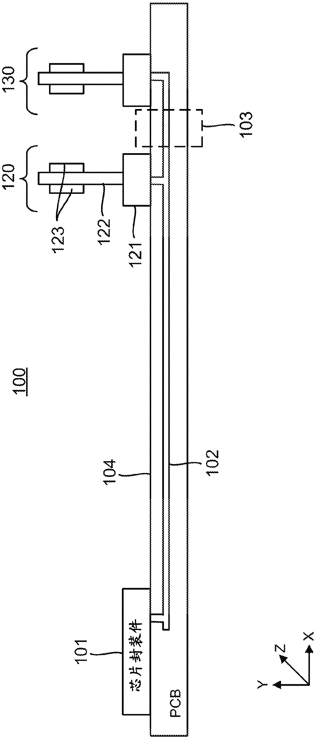
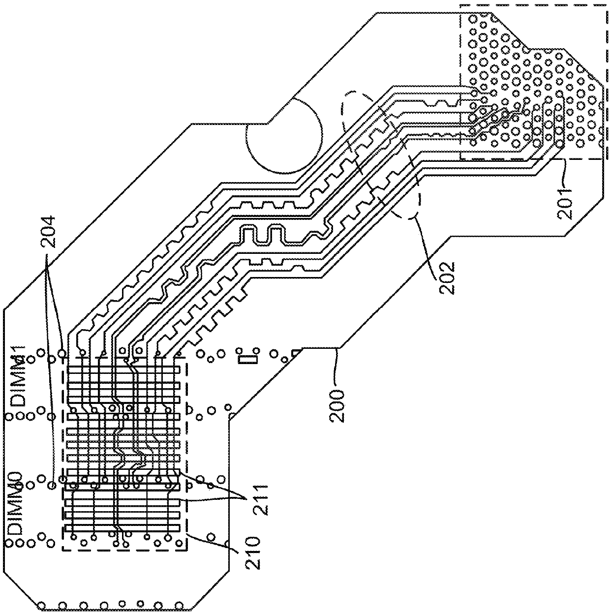
[0020] Various embodiments relate to circuits and methods for increasing signal integrity at electrical couplings between memory modules. For example, example embodiments include a first dual in-line memory module (DIMM) and a second DIMM module mounted to a PCB. The PCB itself may include a topmost ground plane, a middle layer with daisy-chained metal traces coupling the first and second DIMM modules to the processing device. The first DIMM module and the second DIMM module can be placed on the same trace so that the processing device only communicates with one DIMM module at a time.

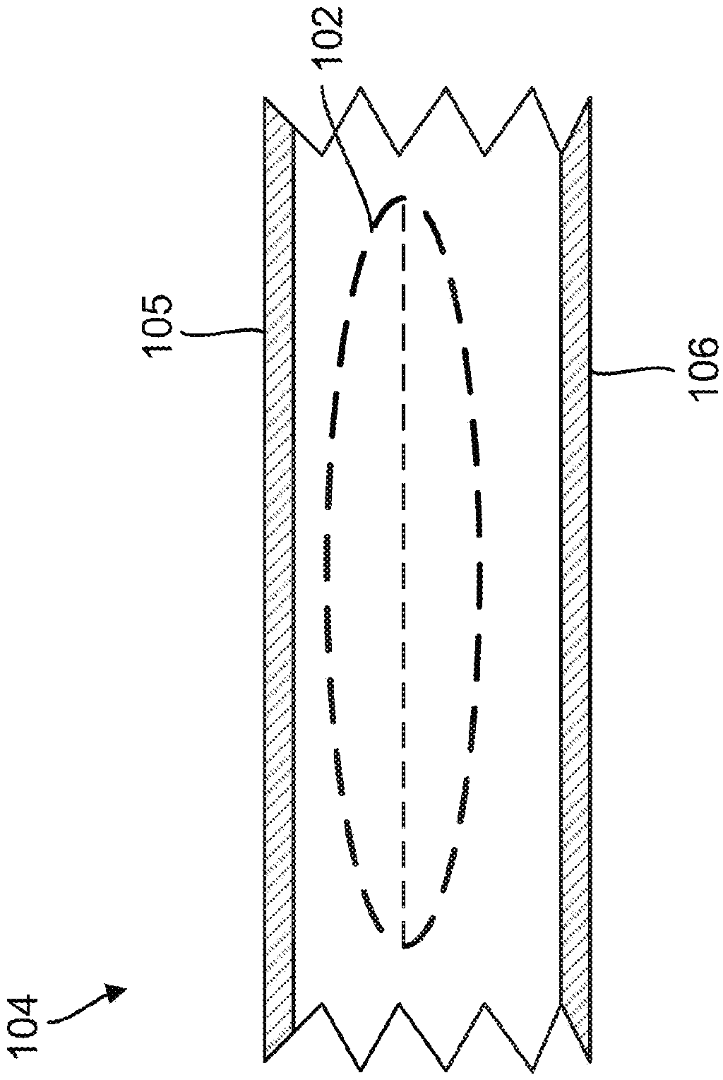
[0021] The PCB can also include a lower ground plane in a layer below the traces. The layers in the PCB can be arranged such that the lower ground plane layer and the topmost ground plane layer sandwich the metal traces. One of the ground plane layers may include an electronic bandgap (EBG) structure in a region physically located between the first DIMM module and the second DIMM module. The...


PUM


Abstract

A system includes: a printed circuit board having a plurality of conductive traces; a processing device coupled to the printed circuit board and in electrical communication with the plurality of conductive traces; a first memory module and a second memory module in electrical communication with the plurality of conductive traces and sharing channels of the conductive traces, wherein the first memory module is physically more proximate to the processing device than is the second memory module; and an electronic band gap (EBG) structure physically disposed in an area between the first memory module and the second memory module.

Description

[0001] Cross References to Related Applications [0002] This application claims priority and benefit to U.S. Nonprovisional Application No. 15 / 659,187, filed July 25, 2017, and U.S. Provisional Patent Application No. 62 / 367,836, filed July 28, 2016, the disclosures of which The content is hereby incorporated by reference in its entirety as if fully set forth below and for all applicable purposes. technical field [0003] The present application relates to memory module electrical couplings, and in particular to electronic bandgap (EBG) structures where memory modules are electrically coupled. Background technique [0004] Some conventional systems include one or more processor chips mounted to a printed circuit board (PCB) and in communication with memory modules. Thus, in one example, a processor chip is mounted on a PCB and communicates with the memory modules through traces in the PCB. During normal operation, the processor issues read and write requests to memory. ...

Claims


Application Information

Patent Timeline
IPC IPC(8): H05K1/02G06F13/40
CPCG06F13/4086H05K1/0225H05K1/025H05K1/0253H05K2201/029H05K2201/09727H05K2201/10159H05K1/0236H01L23/5227H01L23/5286H05K1/0213H05K1/0298
Inventor P·帕特马纳坦
Owner QUALCOMM INC
Why Eureka
Try Eureka