Ultra-wideband switching absorber based on PIN diode

A technology of PIN diodes and absorbers, applied in the field of ultra-broadband switchable absorbers, to achieve the effect of wide coverage of the working frequency band and simple feeding methods

Inactive Publication Date: 2019-04-05
NAT UNIV OF DEFENSE TECH
View PDF3 Cites 9 Cited by
  • Summary
  • Abstract
  • Description
  • Claims
  • Application Information

AI Technical Summary

Problems solved by technology

At present, the existing switch-type absorbers can only switch and switch the whole working frequency band, and in some occasions, only hope to absorb part of the frequency bands, and reflect the rest of the frequency bands.

Method used


Image

  • Ultra-wideband switching absorber based on PIN diode
  • Ultra-wideband switching absorber based on PIN diode
  • Ultra-wideband switching absorber based on PIN diode

Examples


Embodiment Construction

[0021] The present invention will be further described below in conjunction with drawings and embodiments.

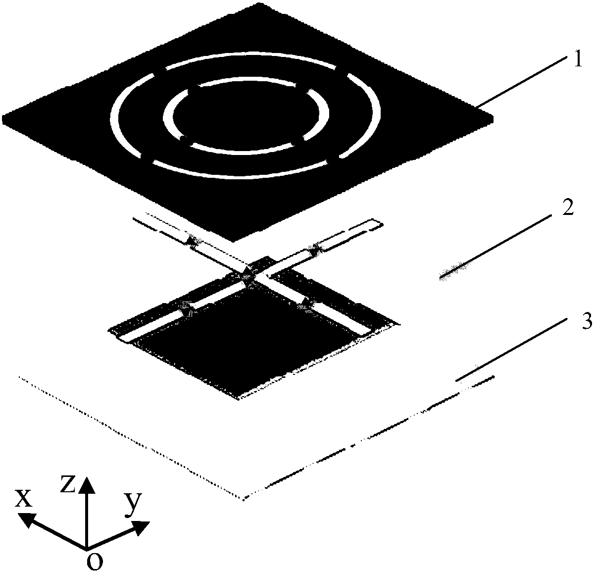
[0022] The present invention provides an ultra-broadband switchable wave absorber based on PIN diodes, which are wave absorbing layer 1, switch layer 2 and bottom plate layer 3 from top to bottom; the wave absorber has a periodic structure, and the periodic unit structure is as follows figure 1 shown.

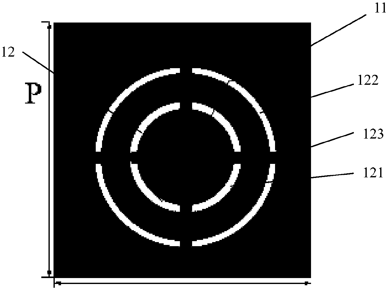
[0023] The absorbing layer 1 is composed of a first dielectric substrate 11 and a plurality of split resonant ring structures 12 periodically attached to the upper surface of the first dielectric substrate; in the embodiment, the first dielectric substrate adopts an FR4 substrate (dielectric constant 4.4, loss angle Tangent 0.007), different types of substrate materials with a dielectric constant range of 4.0-5.0 can also be substituted, and the thickness of the first dielectric substrate is 0.5mm

[0024] Such as figure 2 As shown, the split resonant ring structure 1...


PUM


Abstract

The invention belongs to the technical field of materials, and in particular relates to an ultra-wideband switching absorber based on a PIN diode. The absorber comprises a microwave absorption layer,a switching layer and a bottom plate layer in order from top to bottom; the microwave absorption layer is formed by a first dielectric substrate and a plurality of open resonant ring structures periodically attached to the upper surface of the first dielectric substrate; the switching layer is formed by a second dielectric substrate, a plurality of metal horizontal strips attached to the upper surface of the second dielectric substrate and loading a diode and a plurality of metal vertical strips attached to the lower surface of the second dielectric substrate and loading the diode, wherein themetal horizontal strips are parallel to one another, the metal vertical strips are parallel to one another, and the metal horizontal strips and the metal vertical strips are mutually vehicle in the space direction; and the bottom plate layer is a metal material layer. The ultra-wideband switching absorber based on the PIN diode achieves ultra-wideband microwave absorption from S wave band to an Xwave band, and the working frequency band is wide in coverage; and the ultra-wideband switching absorber has partial frequency band switching feature, is simple in feed mode and has polarization independence.

Description

technical field [0001] The invention belongs to the technical field of materials, and in particular relates to an ultra-wideband switch-type wave absorber based on a PIN diode. Background technique [0002] Absorbers can effectively absorb electromagnetic waves and inhibit their emission and transmission. It is widely used in technical fields such as mobile phones, electronic equipment, high-frequency equipment, microwave active devices, human body safety protection, communication and navigation system anti-interference, smart walls, etc., and has gradually become a research hotspot. However, due to the limitations of their own properties, traditional absorbing materials cannot meet various application requirements. [0003] A metamaterial is an artificial electromagnetic structure arranged periodically, which has electromagnetic properties that natural materials do not have. Due to the advantages of light weight and good performance, metamaterial absorbers have broad appl...

Claims


Application Information

Patent Timeline
Patent Type & Authority Applications(China)
IPC IPC(8): H01Q15/00
CPCH01Q15/002H01Q15/0026
Inventor 虎宁刘培国张继宏毋召锋刘晨曦刘翰青周奇辉戴上凯
Owner NAT UNIV OF DEFENSE TECH
Why Eureka
Try Eureka