A microwave photonic device modeling method based on electromagnetic field and temperature field coupling

A microwave photonic and device modeling technology, applied in the fields of instruments, electrical digital data processing, special data processing applications, etc., can solve problems such as the impact of model accuracy, achieve high-precision device modeling, improve design capabilities and design success rates Effect

Active Publication Date: 2019-04-16
SOUTHWEST CHINA RES INST OF ELECTRONICS EQUIP
View PDF22 Cites 4 Cited by
  • Summary
  • Abstract
  • Description
  • Claims
  • Application Information

AI Technical Summary

Problems solved by technology

However, for the modeling of microwave photonic devices, most of the above techniques only consider a single physical field factor (mainly electromagnetic field)
Although higher accuracy can be obtained in the modeling and simulation of a single device, in the multi-device co-simulation of complex systems, especially in the simulation of highly integrated functional systems, the model accuracy of a single device will be affected. Effects of other physics, such as temperature diffusion and crosstalk

Method used


Image

  • A microwave photonic device modeling method based on electromagnetic field and temperature field coupling
  • A microwave photonic device modeling method based on electromagnetic field and temperature field coupling
  • A microwave photonic device modeling method based on electromagnetic field and temperature field coupling

Examples


Embodiment Construction

[0020] The present invention will be further described below in conjunction with the accompanying drawings.

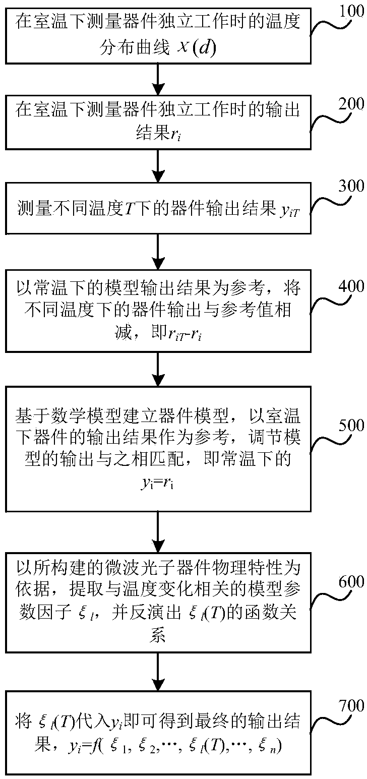
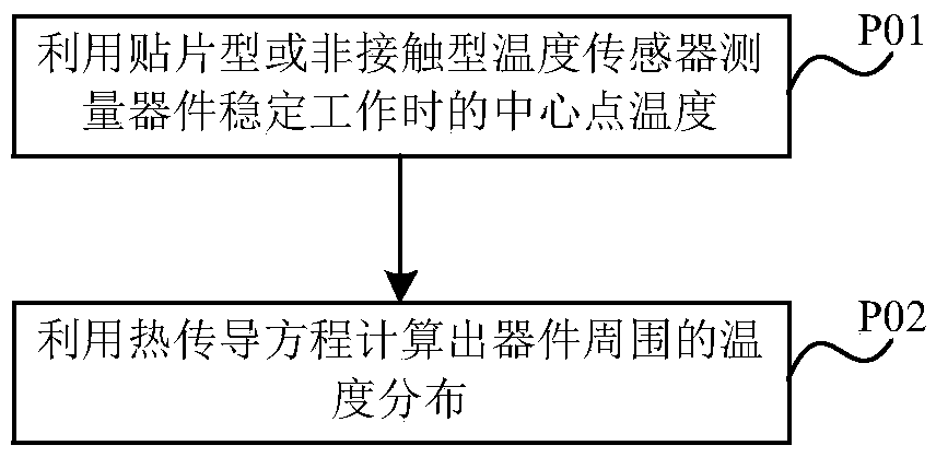
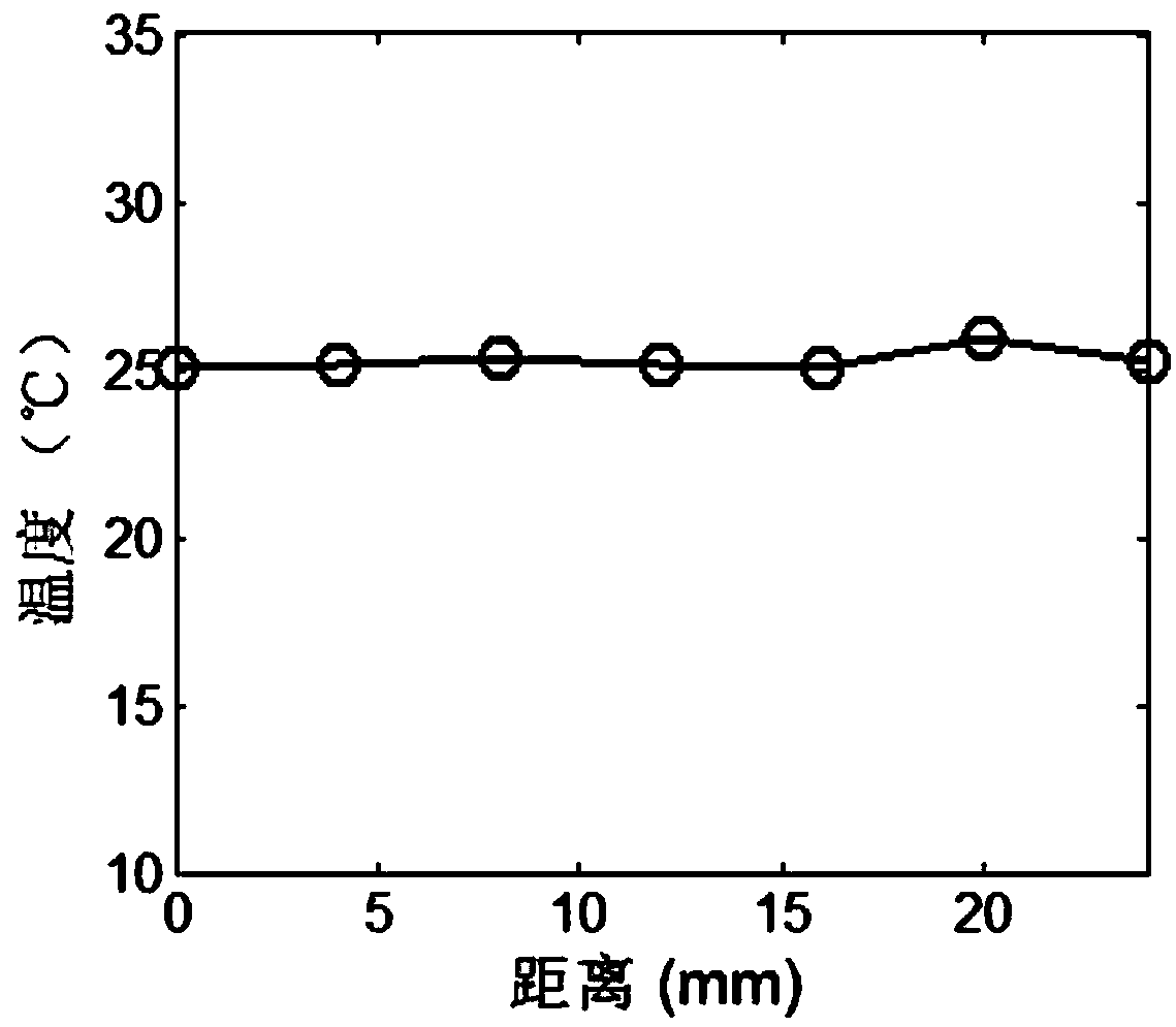
[0021] Such as figure 1 As shown, a microwave photonic device modeling method based on the coupling of electromagnetic field and temperature field includes: step S1, measuring the temperature distribution curve of the device at room temperature when it works independently; step S2, measuring the output of the device at room temperature when it works independently result r i , where i is the sampling point; the measurement result is the result of the device being in the best working state, not affected by temperature changes, and can be established according to the mathematical model; step S3, measuring the device output results r at different temperatures T iT ; Step S4, taking the output results of independent work at room temperature as a reference, subtracting the device output results at different temperatures from the reference value, i.e. r iT -r i , to obtain...


PUM


Abstract

The invention relates to the field of modeling of integrated devices, and discloses a microwave photonic device modeling method based on electromagnetic field and temperature field coupling. The method comprises the following steps: measuring a temperature distribution curve of a device during independent work and an output result ri during independent work at room temperature; Measuring device output results riT at different temperatures T; Taking an output result which works independently at room temperature as a reference to obtain the influence of the temperature on the output result of the device; Establishing an ideal mathematical model output by the device, and adjusting parameters to enable an output result of the mathematical model to be the same as an output result independentlyworking at room temperature; Extracting a temperature factor Xi in the mathematical model and the influence of the temperature on the output result of the device, and inverting a function relation Xi(T) between the temperature factor and the temperature; And substituting the temperature factor Xi and the function relationship Xi (T) into the mathematical model to complete the calculation of the model output characteristic. Aiming at the field of high-integration modeling and simulation, the influence of temperature on the modeling precision of the device can be solved, the modeling speed is high, and the precision is high.

Description

technical field [0001] The invention relates to the field of modeling of integrated devices, in particular to a modeling method for microwave photonic devices based on electromagnetic field and temperature field coupling. Background technique [0002] Device electromagnetic field modeling is the basis for the design and analysis of highly integrated systems. An ideal component model can not only correctly represent the physical characteristics of components, but also be suitable for running numerical solutions in the computer. In recent years, with the rapid development of integrated circuit technology, the feature size of devices and systems has been continuously reduced, and their power density has doubled. The performance of the device and even the entire integrated system will be seriously affected. Therefore, in order to integrate and improve the stability of the system, the temperature characteristics of the devices used should be analyzed at the beginning of the des...

Claims


Application Information

Patent Timeline
Patent Type & Authority Applications(China)
IPC IPC(8): G06F17/50
CPCG06F30/367
Inventor 陈智宇钟欣周涛刘静娴王茂汶
Owner SOUTHWEST CHINA RES INST OF ELECTRONICS EQUIP
Why Eureka
Try Eureka