Thin film transistor structure and measurement method of channel resistance and contact resistance
A thin film transistor and contact resistance technology, which is used in grounding resistance measurement, resistance/reactance/impedance measurement, semiconductor/solid-state device testing/measurement, etc. question
- Summary
- Abstract
- Description
- Claims
- Application Information
AI Technical Summary
Problems solved by technology
Method used
Image

Examples
Embodiment Construction
[0036] In order to further illustrate the technical means adopted by the present invention and its effects, the following describes in detail in conjunction with preferred embodiments of the present invention and accompanying drawings.
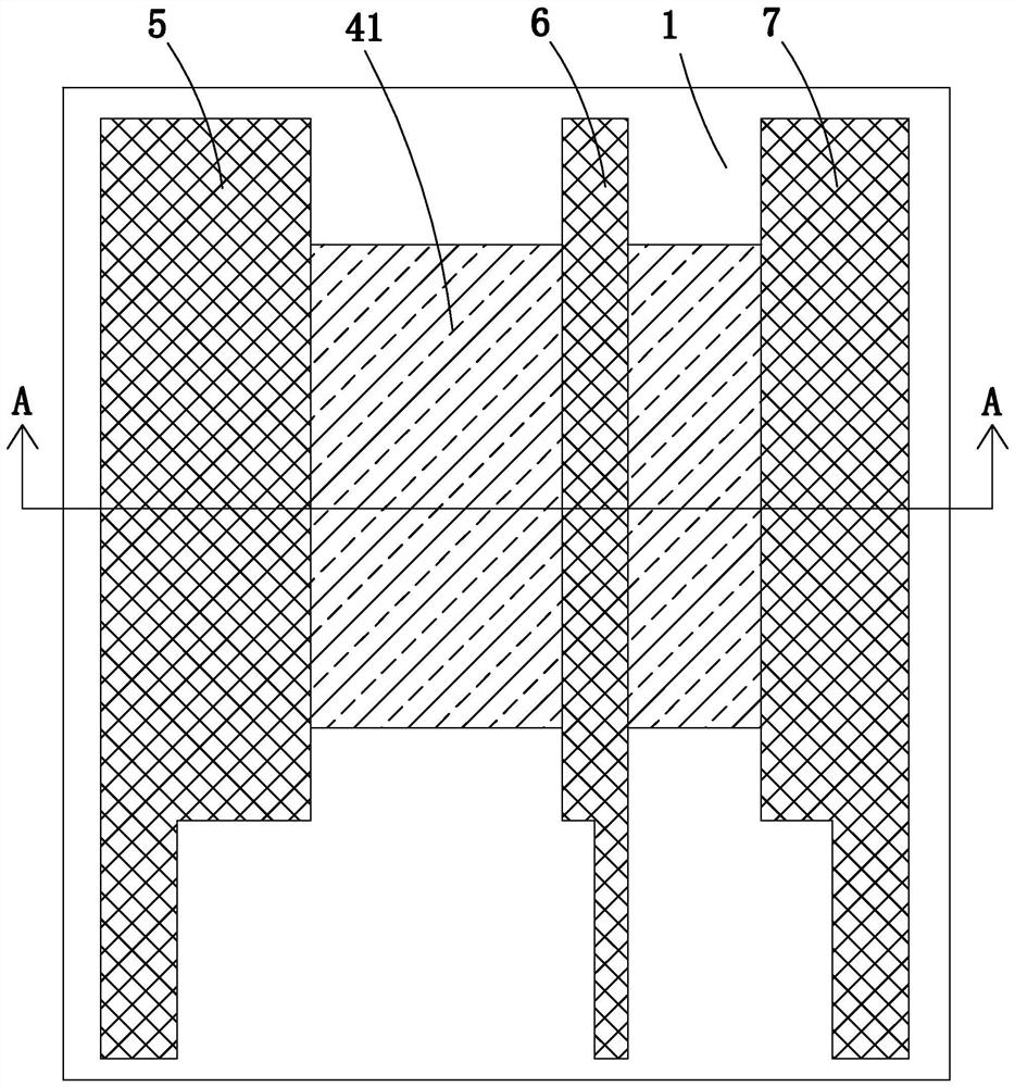
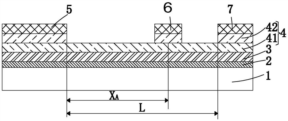
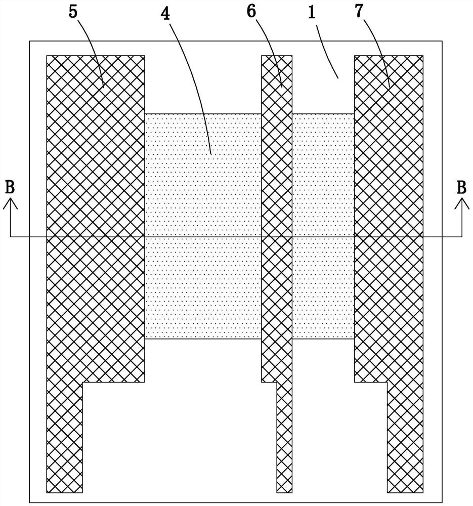
[0037] see figure 1 with figure 2 or image 3 with Figure 4 , the present invention provides a thin film transistor structure, comprising: a substrate 1, a gate 2 disposed on the substrate 1, a gate insulating layer 3 disposed on the gate 2, a gate insulating layer 3 disposed on the The active layer 4 on the gate insulating layer 3 and the source electrode 5, the measuring electrode 6 and the drain electrode 7 arranged at intervals in sequence on the active layer 4;
[0038] The distance between the measuring electrode 6 and the source 5 is different from the distance between the measuring electrode 6 and the drain 7 .
[0039] Specifically, the thin film transistor structure of the present invention is conducive to measuring channel res...
PUM
 Abstract
Description
Claims
Application Information
 - R&D
- Intellectual Property
- Life Sciences
- Materials
- Tech Scout
- Unparalleled Data Quality
- Higher Quality Content
- 60% Fewer Hallucinations
Browse by: Latest US Patents, China's latest patents, Technical Efficacy Thesaurus, Application Domain, Technology Topic, Popular Technical Reports.
© 2025 PatSnap. All rights reserved.Legal|Privacy policy|Modern Slavery Act Transparency Statement|Sitemap|About US| Contact US: help@patsnap.com