A kind of graphene photodetector and preparation method thereof

A photodetector and graphene technology, applied in the field of photodetectors, can solve the problems of complex preparation process, low detection responsivity, and high cost, and achieve the effects of simple structure preparation process, enhanced interaction, and improved detection responsivity

Active Publication Date: 2020-05-05
WUHAN POST & TELECOMM RES INST CO LTD +1
View PDF3 Cites 0 Cited by
  • Summary
  • Abstract
  • Description
  • Claims
  • Application Information

AI Technical Summary

Problems solved by technology

[0004] At present, detectors based on these material systems have achieved good performance and have been commercialized, but there are still shortcomings, such as low detection responsivity, low bandwidth, complex preparation process, and high cost.

Method used


Image

  • A kind of graphene photodetector and preparation method thereof
  • A kind of graphene photodetector and preparation method thereof
  • A kind of graphene photodetector and preparation method thereof

Examples


Embodiment Construction

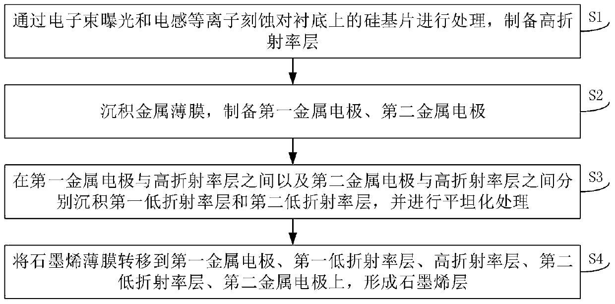
[0033] The present invention will be described in further detail below in conjunction with the accompanying drawings and embodiments.

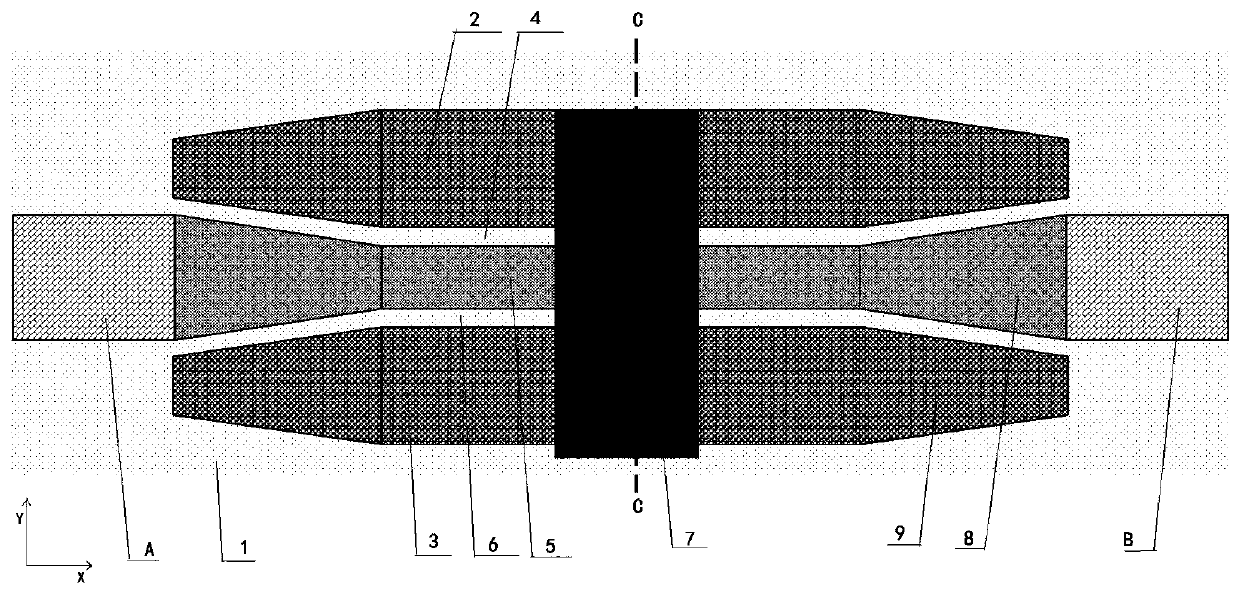
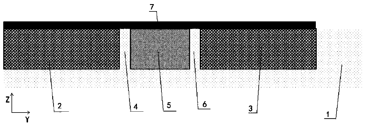
[0034] see figure 1 As shown, the embodiment of the present invention provides a graphene photodetector, which includes a substrate 1, an optical input terminal A and an optical output terminal B, and an optical waveguide structure, and the length, width and height direction of the substrate 1 are defined as X , Y, Z directions, see figure 1 and figure 2 shown;

[0035] see figure 1 As shown, the light input terminal A and the light output terminal B are arranged on the substrate 1 at intervals along the X direction;

[0036] The optical waveguide structure is located between the optical input end A and the optical output end B, and the optical waveguide structure includes two parts:

[0037] The first part: the first metal electrode 2, the refractive index layer and the second metal electrode 3 arranged on the substrate 1, the first met...


PUM

PropertyMeasurementUnit
sizeaaaaaaaaaa
sizeaaaaaaaaaa
sizeaaaaaaaaaa

Abstract

The invention discloses a graphene photodetector and a preparation method thereof. The graphene photodetector comprises a substrate, a light input end, a light output end and an optical waveguide structure, wherein the directions of length, width and height of the substrate are respectively defined as X, Y and Z directions; the light input end and the light output end are arranged on the substrateat intervals in the X direction; the optical waveguide structure is located between the light input end and the light output end, and the optical waveguide structure comprises a first metal electrode, a refractive index layer and a second metal electrode that are arranged on the substrate and a graphene layer arranged on the surface of the high refractive index layer, wherein the first metal electrode, the refractive index layer and the second metal electrode are sequentially arranged and connected in the Y direction; the refractive index layer comprises a first low refractive index layer, ahigh refractive index layer and a second low refractive index layer which are sequentially arranged and connected in the Y direction, two ends of the high refractive index layer are respectively connected with the light input end and the light output end, and two ends of the graphene layer extend along the Y direction to respectively cover the first metal electrode and the second metal electrode.According to the scheme of the invention, the detection responsiveness and the photoelectric detection bandwidth can be improved.

Description

technical field [0001] The invention relates to the technical field of photodetectors, in particular to a graphene photodetector and a preparation method thereof. Background technique [0002] In optoelectronic integrated circuits, the optical detector is one of the core integrated devices at the receiving end, which converts high-speed optical data into electrical signals. Optical detectors use materials with pyroelectric effect, photoelectric effect, and electroabsorption effect to detect the amplitude of light. Commonly used material systems include III-V materials (InP) and silicon germanium (Si / Ge). [0003] As a new type of material, graphene has excellent optoelectronic properties, such as broadband photoresponse, strong interaction with light, ultrafast carrier mobility, etc., combined with the optical waveguide structure of silicon-based materials, it can realize the ultra-wideband, high-responsivity detection. The basic principle of ultra-broadband, high-respons...

Claims


Application Information

Patent Timeline
Patent Type & Authority Patents(China)
IPC IPC(8): H01L31/09H01L31/028H01L31/18
CPCH01L31/028H01L31/09H01L31/1876Y02P70/50
Inventor 胡晓肖希张宇光陈代高李淼峰王磊冯朋余少华
Owner WUHAN POST & TELECOMM RES INST CO LTD
Why Eureka
Try Eureka