Image sensor signal acquisition method and signal acquisition circuit

An image sensor and signal acquisition technology, applied in the field of image sensors, can solve the problem that processing logic needs to be improved, etc.

Active Publication Date: 2020-11-06
SHANGHAI OXI TECH
View PDF5 Cites 0 Cited by
  • Summary
  • Abstract
  • Description
  • Claims
  • Application Information

AI Technical Summary

Problems solved by technology

[0005] The processing logic of the existing signal acquisition method needs to be improved when clearing the pixels

Method used


Image

  • Image sensor signal acquisition method and signal acquisition circuit
  • Image sensor signal acquisition method and signal acquisition circuit
  • Image sensor signal acquisition method and signal acquisition circuit

Examples


Embodiment Construction

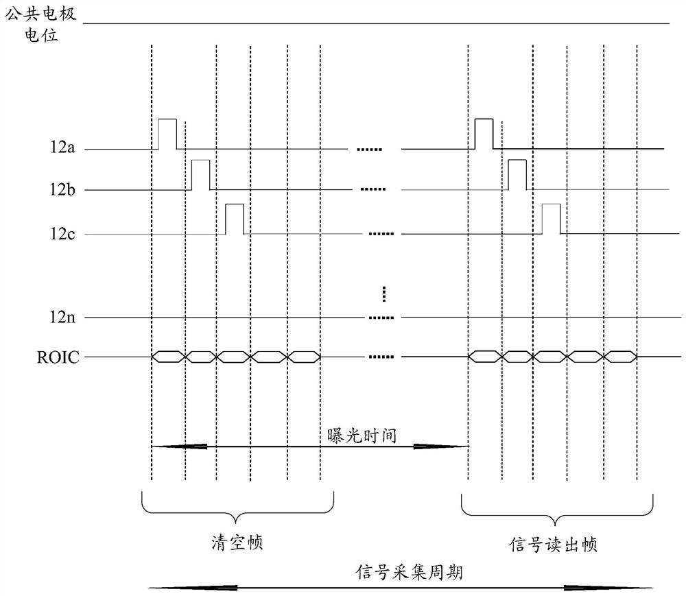
[0030] As mentioned in the background art, the processing logic of the existing signal acquisition method needs to be improved when clearing pixels.

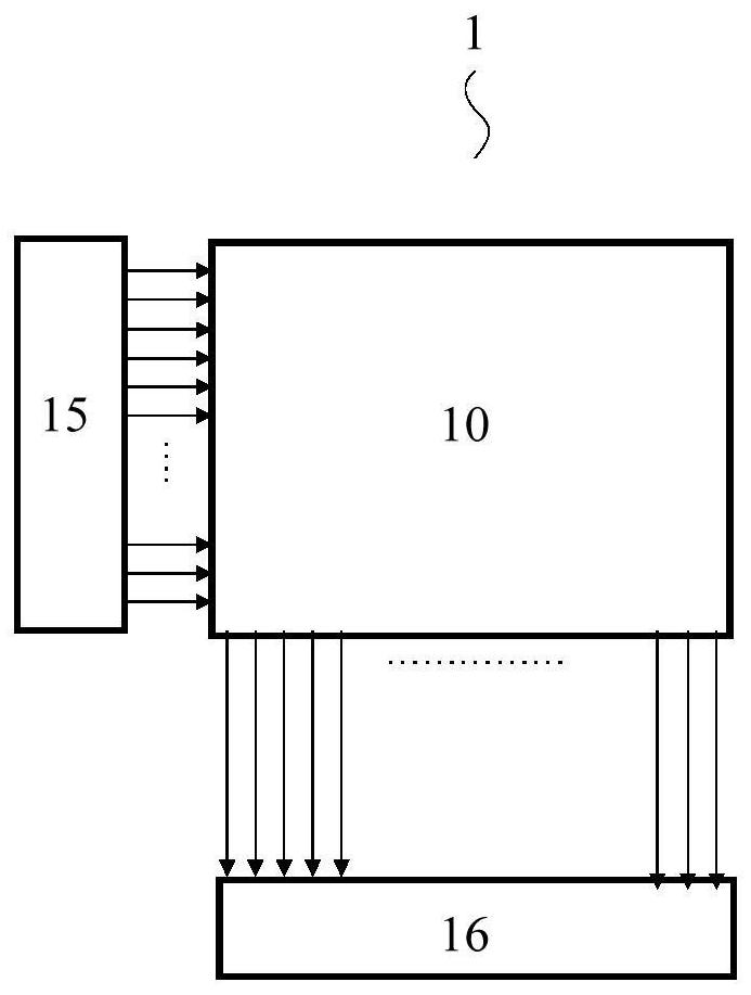
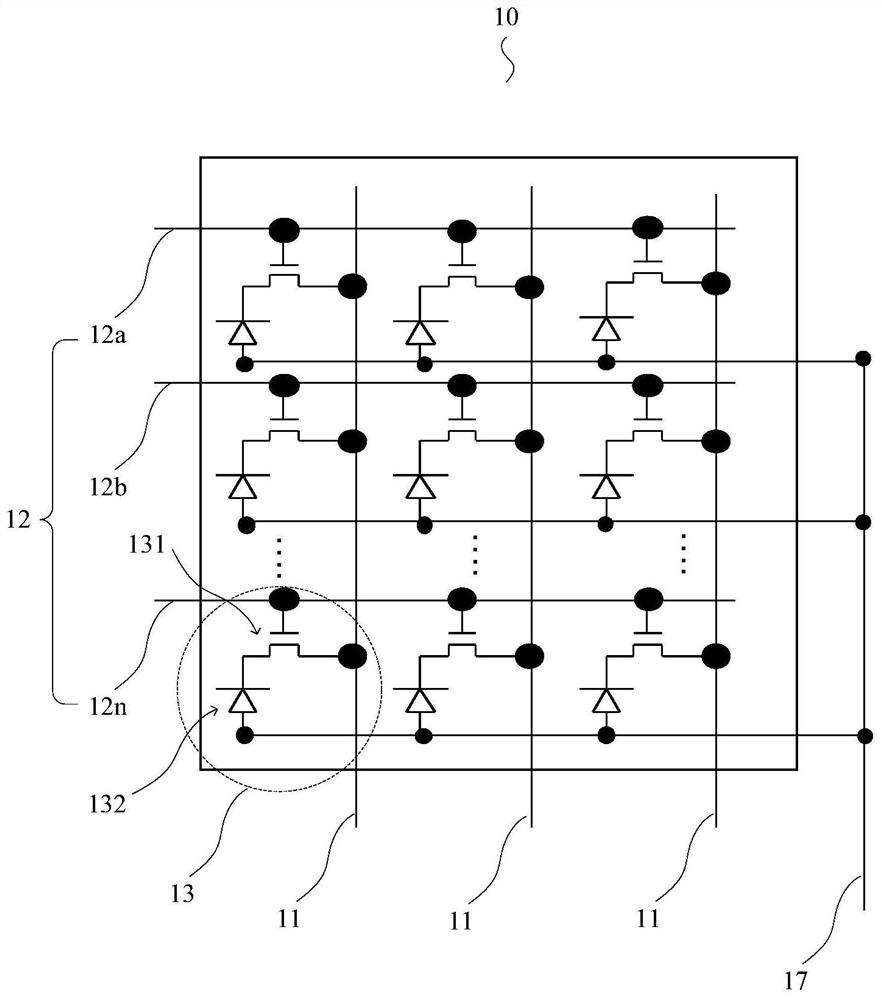
[0031] Specifically, refer to figure 1 and figure 2 The signal acquisition circuit 1 of the image sensor may include a pixel array 10 , a scan line control circuit 15 and a signal readout chip 16 (Readout IC, ROIC for short). Wherein, the pixel array 10 has a plurality of data lines 11 and a plurality of scan lines 12 , the data lines 11 and the scan lines 12 define grids arranged in an array, and the areas where the grids are located correspond to pixels 13 .

[0032] Further, the pixel 13 includes at least one pixel switch 131 and at least one photosensitive device 132 . Wherein, the pixel switch 131 is generally a thin film transistor (Thin Film Transistor, TFT for short) device, and the photosensitive device 132 is used to collect an externally input optical signal and convert it into an electrical signal, and then store ...


PUM


Abstract

A signal acquisition method and signal acquisition circuit of an image sensor, the image sensor includes a plurality of pixels arranged in an array, each pixel includes a photodiode, and the signal acquisition method includes: in each signal acquisition cycle , performing signal acquisition on the plurality of pixels row by row, the signal acquisition period includes at least one reset frame and at least one clear frame, wherein, in each reset frame, to each of the collected pixels A forward bias is applied to the photodiodes; and a reverse bias is applied to the photodiodes of each of the pixels being collected in each of the blanking frames. The solution provided by the invention can shorten the signal acquisition period while ensuring a better clearing effect and eliminating the influence of ambient light on imaging.

Description

technical field [0001] The present invention relates to the technical field of image sensors, in particular to a signal acquisition method and a signal acquisition circuit of an image sensor. Background technique [0002] An image sensor is a sensing device that uses the photoelectric conversion function of a photoelectric device to convert the light image on the photosensitive surface into an electrical signal that is proportional to the light image. [0003] Taking an optical fingerprint sensor as an example, it usually consists of a pixel array, a control line (also called a drive line), a scan line (also called a signal readout line), and the like. Wherein, each pixel in the pixel array has a photoelectric device to realize the conversion of optical signal to electrical signal. [0004] The existing optoelectronic devices used in image sensors are usually photodiodes (Photo-Diodes). Prior to acquisition, unwanted charges are present on each pixel. Therefore, before th...

Claims


Application Information

Patent Timeline
Patent Type & Authority Patents(China)
IPC IPC(8): H04N5/235H04N5/378H04N5/369
CPCH04N23/73H04N25/70H04N25/75
Inventor 凌严朱虹
Owner SHANGHAI OXI TECH
Why Eureka
Try Eureka