MEMS chip structure and preparation method, mask plate, and device

A chip structure and device technology, applied in the direction of microstructure technology, microstructure device, manufacturing microstructure device, etc., can solve the problem of large device volume

Pending Publication Date: 2019-04-19
全普半导体科技(深圳)有限公司
View PDF0 Cites 0 Cited by
  • Summary
  • Abstract
  • Description
  • Claims
  • Application Information

AI Technical Summary

Problems solved by technology

In traditional devices, each peripheral circuit occupies a single circuit board, and is electrically c

Method used


Image

  • MEMS chip structure and preparation method, mask plate, and device
  • MEMS chip structure and preparation method, mask plate, and device
  • MEMS chip structure and preparation method, mask plate, and device

Examples


Embodiment Construction

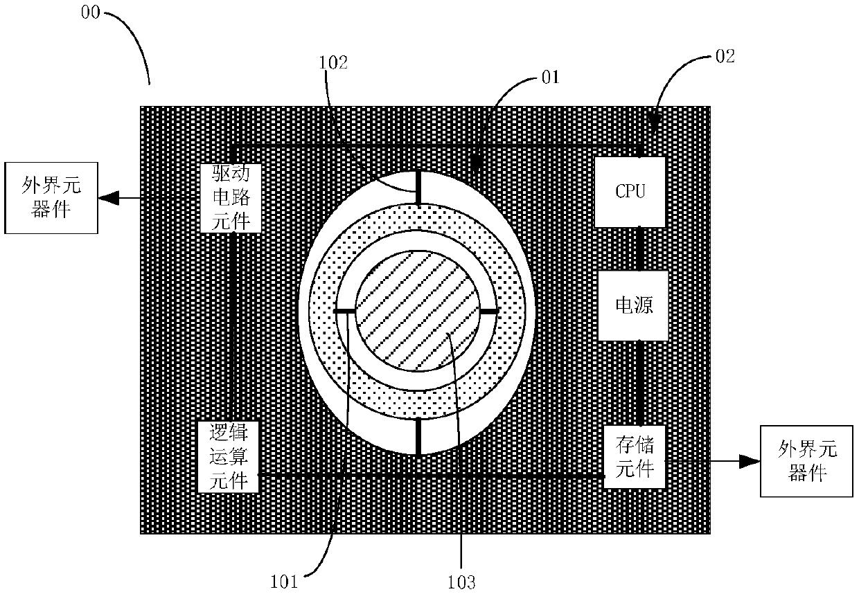
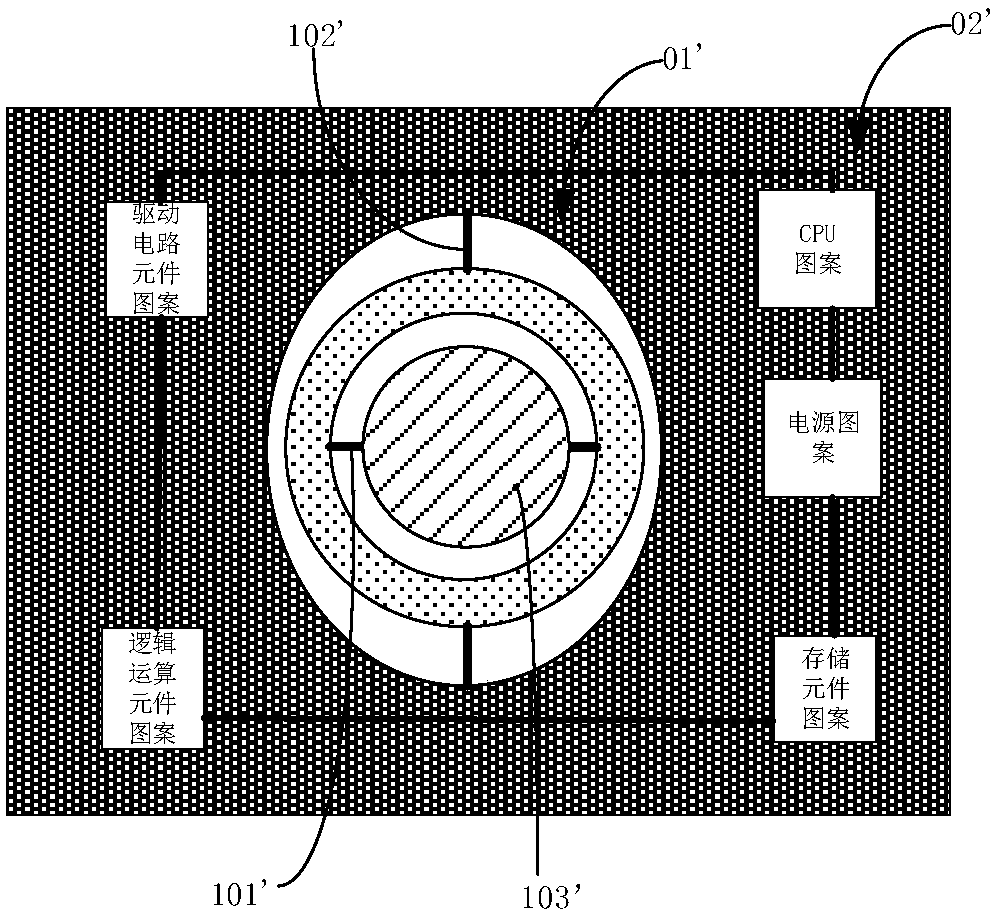
[0071] In order to make the content of the present invention clearer and easier to understand, the content of the present invention will be further described below in conjunction with the accompanying drawings. Of course, the present invention is not limited to this specific embodiment, and general replacements known to those skilled in the art are also covered within the protection scope of the present invention.

[0072] The following is attached Figure 1~6 The present invention will be described in further detail with specific examples. It should be noted that the drawings are all in a very simplified form, using imprecise scales, and are only used to facilitate and clearly achieve the purpose of assisting in describing the present embodiment.

[0073] see figure 1 , a MEMS chip structure in this embodiment, the MEMS main element 01 and the MEMS auxiliary element 02 are both on the same chip 00 .

[0074] The MEMS master element 01 is used to reflect the light beam and ...


PUM


Abstract

The invention provides a MEMS chip structure and a preparation method, a mask plate, and a device. By arranging a MEMS main element and MEMS auxiliary elements, a driving circuit element, a logic operation element, a CPU central processing element, a power supply and the MEMS main element are integrated on the same chip, the condition that multiple processing circuit boards in the traditional MEMSdevice occupy large and more space, and the volume of the device based on the MEMS is obviously reduced; namely, a periphery circuit design is removed, the traditional chip periphery circuit is unnecessary by adopting the MEMS chip structure of the invention; the volume and the occupied space of the electric device product taking the MEMS chip structure disclosed by the invention as the basis aregreatly reduced since the chip periphery circuit occupies the main space and volume of the electric device product, and the miniaturization and the portability of the electric device are really realized.

Description

technical field [0001] The invention relates to the technical field of semiconductors, in particular to a MEMS chip structure and a preparation method thereof, as well as a mask plate and a MEMS device. Background technique [0002] A traditional MEMS chip includes a scanning micromirror and a scanning platform. In addition, a peripheral circuit board is arranged on the periphery of the MEMS chip structure, and the peripheral circuit is electrically connected to the MEMS chip structure, and the peripheral circuit includes a controller circuit and the like. In the MEMS chip structure, the scanning micromirror is coupled to the scanning platform. The scanning platform can move under the action of driving excitation and magnetic field, and the controller controls the moving direction and position of the scanning platform. The scanning micromirror is capable of rotating along the axis of rotation. In traditional devices, each peripheral circuit occupies a single circuit board...

Claims


Application Information

Patent Timeline
IPC IPC(8): B81B7/02B81C1/00
CPCB81B7/02B81C1/00246B81C1/00404
Inventor 汪际军
Owner 全普半导体科技(深圳)有限公司
Why Eureka
Try Eureka