Adder unit and display device

A technology for adders and displays, applied in instruments, static indicators, etc., can solve the problems of reduced pixel drive time, increased power consumption, and decreased display accuracy, to reduce threshold voltage drift, increase output time, and improve display accuracy. Effect

Active Publication Date: 2019-04-19
PEKING UNIV SHENZHEN GRADUATE SCHOOL
View PDF6 Cites 1 Cited by
  • Summary
  • Abstract
  • Description
  • Claims
  • Application Information

AI Technical Summary

Problems solved by technology

For traditional adders, the output stage op amp often has voltage mismatch, capacitor mismatch, etc., which affects the output accuracy
At the same time, in terms of timing, the output of the traditional capacitive sampling adder will be in a high-impedance state during the sampling phase, so there is no output signal at the output of the source drive circuit during the sampling phase, resulting in a reduction in the driving time of the pixel or restricted
For display circuits, reducing or limiting the driving time of pixels means that the display accuracy under the same driving capability is reduced, or a larger driving circuit is used to achieve the same accuracy, resulting in increased power consumption

Method used


Image

  • Adder unit and display device
  • Adder unit and display device
  • Adder unit and display device

Examples


no. 1 example

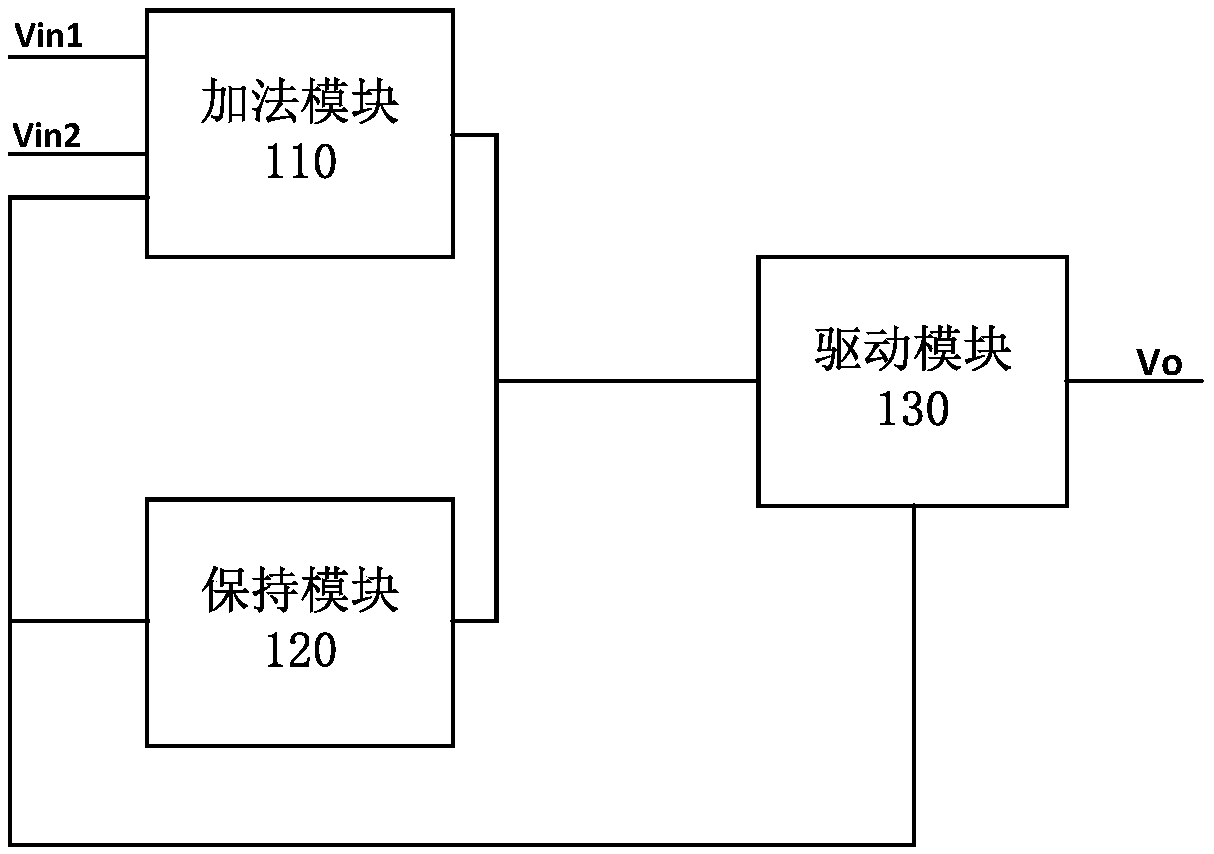
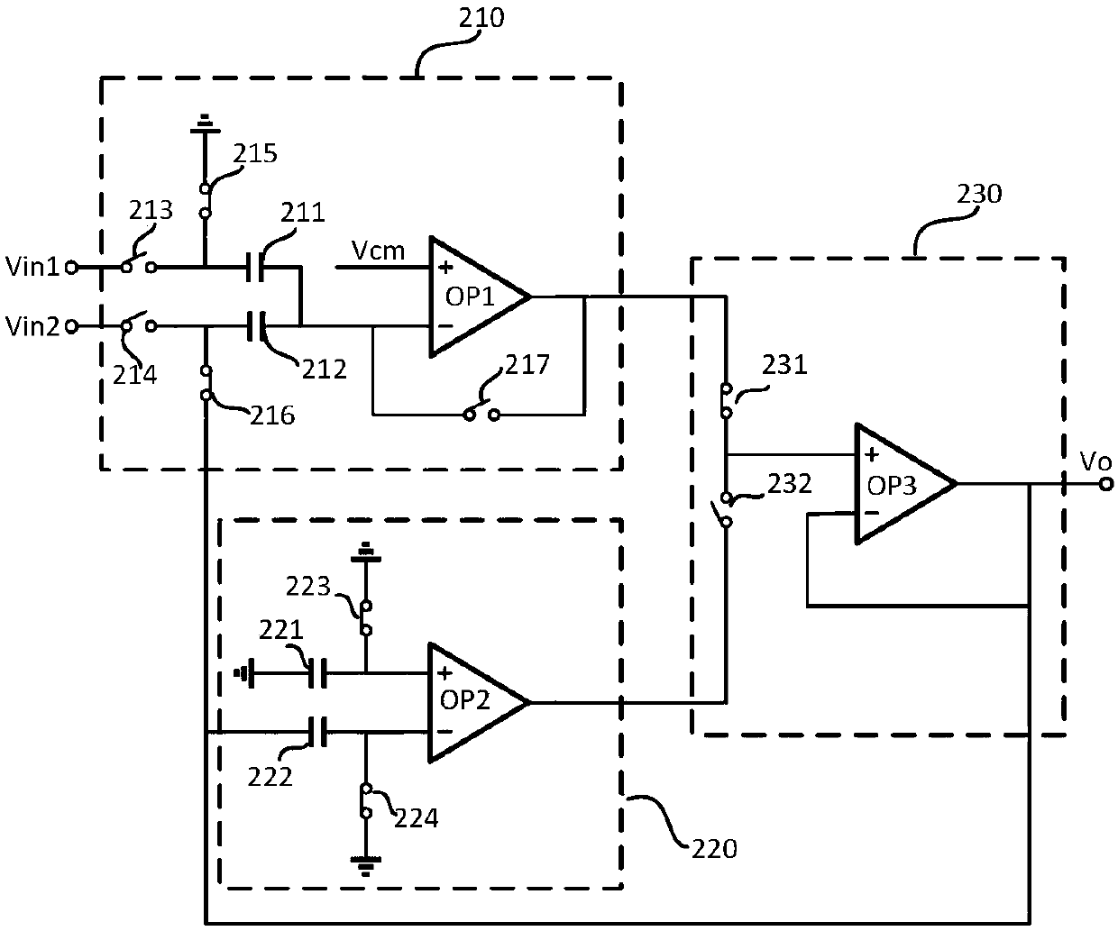
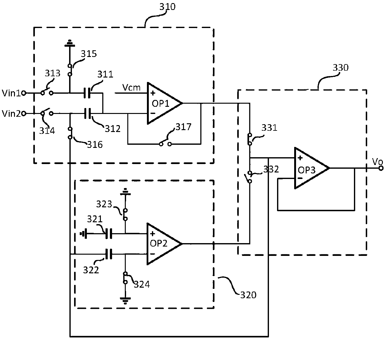
[0056] Compared with the first embodiment, the output terminal (or negative input terminal) of the driving module 330 in this embodiment is not coupled to the input terminals of the adding module 310 and the holding module 320 . The positive input terminal of the driving module 330 is coupled to the negative input terminals of the adding module 310 and the holding module 320 through capacitors 312 and 322 respectively.

[0057] After the above configuration, during the sampling phase, the output terminal of the holding module 320 is coupled to the negative input terminal to form negative feedback; during the holding phase, the output terminal of the adding module 310 is coupled to its negative input terminal via the switch 316 to form negative feedback.

[0058] Figure 3b It is an input and output timing diagram of the adder unit according to the second embodiment of the present application. Figure 3b The timing in the same applies to figure 2 middle adder unit.

[0059]...


PUM


Abstract

The invention provides a display source driving circuit, comprising an adder unit addition module, configured to perform sampling on a plurality of input signals within a first time period under the influence of a clock signal; a holding module, configured to provide a holding signal within the first time period under the influence of the clock signal; and a driving module, configured to generatea first output signal based on the holding signal within the first time period, and generate a second output signal based on a superposed signal of the plurality of input signals within a second timeperiod; wherein the plurality of input signals at least comprise a data signal and a compensation signal, and the first time period and the second time period are adjacent time periods in the clock signal. By adoption of the display source driving circuit of the adder unit provided by the invention, the input signals can be superposed on an analog domain, so that the display precision is effectively improved.

Description

technical field [0001] The application belongs to the field of information display, and in particular relates to a circuit suitable for display driving of an active matrix organic light-emitting diode with a compensation function. Background technique [0002] The active matrix organic light emitting diode display (Active Matrix Organic Light Emitting Diode, AMOLED) is driven by the current generated by the thin film field effect transistor in a saturated state to emit light. In the panel production process, due to the instability of the process, the mobility of the thin film field effect transistor will fluctuate greatly. In addition, due to material characteristics, organic light-emitting devices will age after a period of display, and their threshold voltages will drift, resulting in inconsistent output currents when the same gray-scale voltage is input to the source drive circuit of the display. [0003] The current compensation methods are divided into two methods: int...

Claims


Application Information

Patent Timeline
Patent Type & Authority Applications(China)
IPC IPC(8): G09G3/3225G09G3/3291
CPCG09G3/3225G09G3/3291
Inventor 张盛东邱赫梓廖聪维郭凡林兴武鲁文高张敏
Owner PEKING UNIV SHENZHEN GRADUATE SCHOOL
Why Eureka
Try Eureka