Making methods of grid electrode and thin film transistor

A technology for thin film transistors and a manufacturing method, which is applied in semiconductor/solid state device manufacturing, semiconductor devices, electrical components, etc., can solve problems such as affecting the work efficiency of thin film transistors, and achieve the effect of improving work efficiency and avoiding burr structures.

Active Publication Date: 2019-04-23
TCL CHINA STAR OPTOELECTRONICS TECH CO LTD
View PDF8 Cites 0 Cited by
  • Summary
  • Abstract
  • Description
  • Claims
  • Application Information

AI Technical Summary

Problems solved by technology

[0006] In view of this, the present invention provides a method for manufacturing a gate and a thin film transistor to solve the problem of affecting the working efficiency of the thin film transistor in the prior art using a gate with a double-layer structure

Method used


Image

  • Making methods of grid electrode and thin film transistor
  • Making methods of grid electrode and thin film transistor
  • Making methods of grid electrode and thin film transistor

Examples


Embodiment Construction

[0027] The following descriptions of the various embodiments refer to the accompanying drawings to illustrate specific embodiments in which the present invention can be practiced. Furthermore, the directional terms mentioned in the present invention are, for example, up, down, top, bottom, front, back, left, right, inside, outside, side, surrounding, central, horizontal, transverse, vertical, longitudinal, axial, The radial direction, the uppermost layer or the lowermost layer, etc. are only directions referring to the attached drawings. Therefore, the directional terms used are used to illustrate and understand the present invention, but not to limit the present invention.

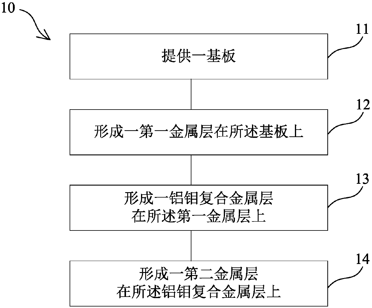
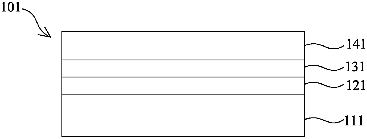
[0028] Please refer to Figure 1A and 1B As shown, the gate manufacturing method 10 according to an embodiment of the present invention mainly includes steps 11 to 14: providing a substrate (step 11); forming a first metal layer on the substrate (step 12); forming an aluminum molybdenum forming a compo...


PUM

PropertyMeasurementUnit
Thicknessaaaaaaaaaa

Abstract

The invention discloses making methods of a grid electrode and a thin film transistor. The making method of the grid electrode comprises the following steps of providing a base plate; forming a firstmetal layer on the base plate; forming an aluminum and molybdenum composite metal layer on the first metal layer; forming a second metal layer on the aluminum and molybdenum composite metal layer so as to form the grid electrode. The making methods of the grid electrode and the thin film transistor provided by the embodiment of the invention have the advantages that the generation of a burr structure of the grid electrode can be reduced or avoided; the work efficiency of the thin film transistor is further improved.

Description

technical field [0001] The invention relates to a semiconductor field, in particular to a method for manufacturing a gate and a thin film transistor. Background technique [0002] In recent years, display technology has developed rapidly, and flat panel displays have replaced bulky CRT displays and are increasingly embedded in people's daily lives. Currently, commonly used flat panel displays include liquid crystal displays (Liquid Crystal Display, LCD) and organic light-emitting diode (Organic Light-Emitting Diode, OLED) displays. The above-mentioned flat-panel display has the characteristics of small size, low power consumption, and no radiation, and occupies a dominant position in the current flat-panel display market. [0003] In the array substrate of the flat panel display, each pixel is equipped with a switching unit for controlling the pixel, that is, a thin film transistor (Thin Film Transistor, TFT), and the TFT at least includes a gate, a source region and a drai...

Claims


Application Information

Patent Timeline
IPC IPC(8): H01L21/28H01L21/44H01L29/423H01L21/336H01L21/34
CPCH01L29/401H01L29/42372H01L29/42384H01L29/66742H01L29/66969
Inventor 王建刚
Owner TCL CHINA STAR OPTOELECTRONICS TECH CO LTD
Why Eureka
Try Eureka