Array substrate and manufacturing method thereof, and display device

An array substrate and array technology, applied in the field of display devices, can solve problems such as difficult bending of the pixel area, and achieve the effects of improving adhesion, facilitating manufacturing process, and improving electrical properties

Inactive Publication Date: 2019-04-23
WUHAN CHINA STAR OPTOELECTRONICS SEMICON DISPLAY TECH CO LTD
View PDF6 Cites 50 Cited by
  • Summary
  • Abstract
  • Description
  • Claims
  • Application Information

AI Technical Summary

Problems solved by technology

[0003] At present, there is no fully flexible display mobile phone on the market, and only partial bending is performed in the bending area. In the flexible OLED display in the prior art, the inorganic film layer is generally etched in the bending area, and the organic photoresist Fill it, this structure is more difficult to bend in the pixel area

Method used


Image

  • Array substrate and manufacturing method thereof, and display device
  • Array substrate and manufacturing method thereof, and display device
  • Array substrate and manufacturing method thereof, and display device

Examples


Embodiment Construction

[0049] The following description of the embodiments refers to the accompanying drawings to illustrate specific embodiments in which the invention may be practiced. The directional terms mentioned in the present invention, such as "up", "down", "front", "back", "left", "right", "top", "bottom", etc., are only for reference to the attached drawings. direction. Therefore, the directional terms used are used to illustrate and understand the present invention, but not to limit the present invention.

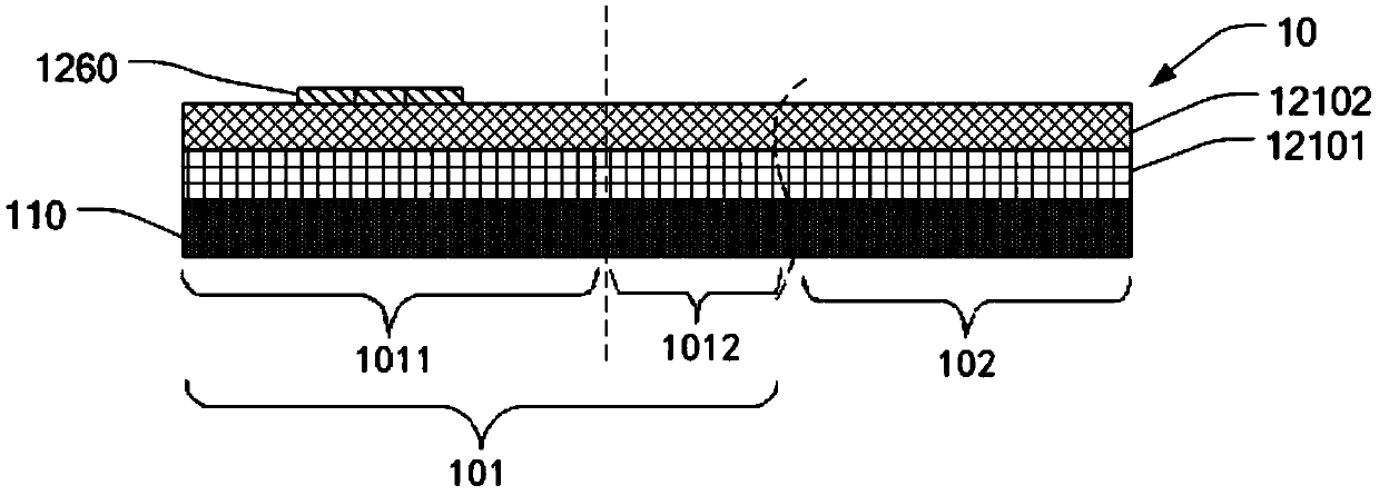
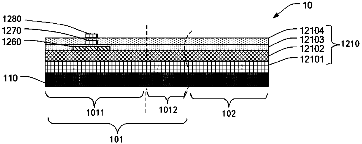
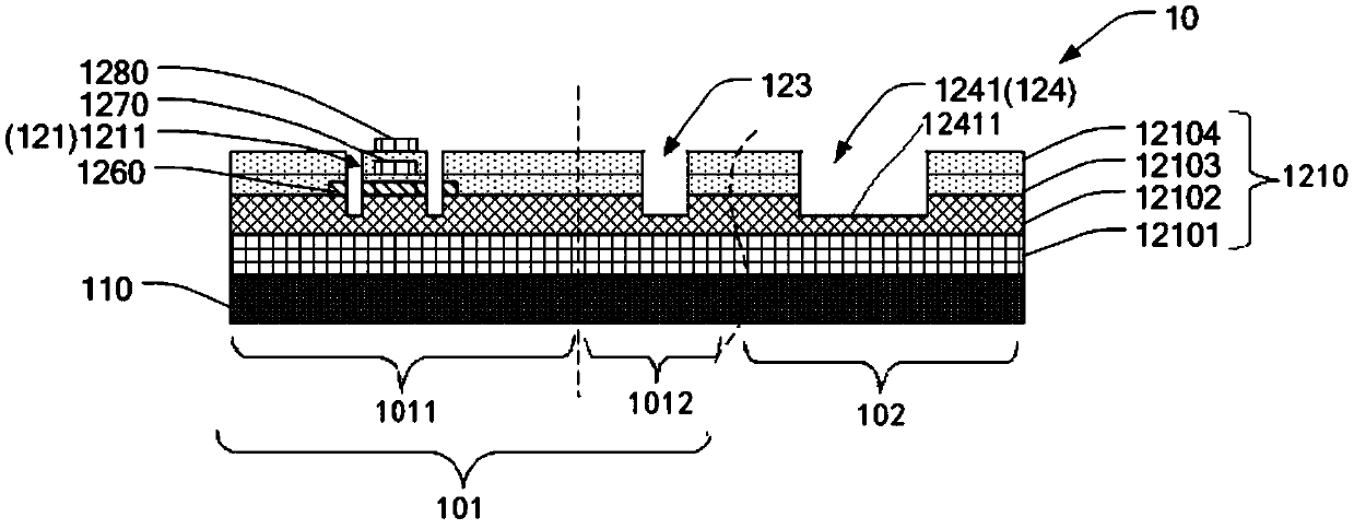
[0050] Such as Figure 10 As shown, in one embodiment, the array substrate 10 of the present invention has a bending area 102 and a pixel area 101 adjacent to the bending area 102, and the pixel area 101 has several pixel unit areas 1011 and is connected to the The non-pixel unit area 1012 of the pixel unit area 1011 .

[0051] The array substrate 10 includes a flexible substrate 110 and an array layer 120 . The array layer 120 covers the flexible substrate 110 . The array layer ...


PUM


Abstract

The invention discloses an array substrate and a manufacturing method thereof, and a display device. The array substrate has a bending area and a pixel area adjacent to the bending area, the pixel area has a plurality of pixel unit areas and a non-pixel unit area connected with the pixel unit area; the array substrate includes: a flexible substrate and an array layer, wherein the array layer includes an array base layer having a first groove and a second groove, the first groove corresponds to the non-pixel unit area in the pixel area, and the second groove corresponds to the bending area; a filling layer filled in the first groove and the second groove; and an organic dielectric layer covering the array base layer and the filling layer, wherein the organic dielectric layer and the fillinglayer employ organic photoresist materials. The array substrate and the manufacturing method thereof, and the display device having the array substrate effectively reduce the stress of each film layer in the array substrate when the film layers are bent so as to achieve bending of the pixel area.

Description

technical field [0001] The present invention relates to the fields of display devices and the like, and specifically relates to an array substrate, a manufacturing method thereof, and a display device. Background technique [0002] OLED (Organic Light-Emitting Diode) display has become the mainstream display trend due to its self-illumination, wide viewing angle, high contrast, fast response and other characteristics. At present, with people's pursuit of the ultimate display experience, full screens and narrow bezels have become development hotspots in the current display field. The flexible OLED display is even more popular and has become a trend. It has many advantages, such as ultra-thin and ultra-light screen, smaller size, more convenient to carry, and stronger customer experience. [0003] At present, there is no fully flexible display mobile phone on the market, and only partial bending is performed in the bending area. In the flexible OLED display in the prior art, ...

Claims


Application Information

Patent Timeline
Patent Type & Authority Applications(China)
IPC IPC(8): H01L27/12H01L27/32G09F9/30
CPCH01L27/124H01L27/1248H01L27/1259H01L27/127G09F9/301H10K59/12
Inventor 胡俊艳
Owner WUHAN CHINA STAR OPTOELECTRONICS SEMICON DISPLAY TECH CO LTD
Why Eureka
Try Eureka