Eureka AIR delivers breakthrough ideas for toughest innovation challenges, trusted by R&D personnel around the world.

Display panel and display device

A display panel and display function technology, applied in static indicators, nonlinear optics, instruments, etc., can solve problems such as uneven image quality, gray scale, and inability to compensate for light brightness

Active Publication Date: 2019-04-26
HEFEI XINSHENG OPTOELECTRONICS TECH CO LTD +1
View PDF10 Cites 2 Cited by
  • Summary
  • Abstract
  • Description
  • Claims
  • Application Information

AI Technical Summary

Problems solved by technology

However, in the manufacturing process, a thick copper process and an oxide process are required, resulting in a large-scale display device that cannot effectively compensate the brightness of light while pursuing high pixel density, and poor diffusion that cannot be recognized by the human eye often occurs. Moreover, when the product quality is displayed, there will be obvious uneven picture quality and poor grayscale, which will affect the user's perception experience.

Method used


Image

  • Display panel and display device
  • Display panel and display device
  • Display panel and display device

Examples


Embodiment 1

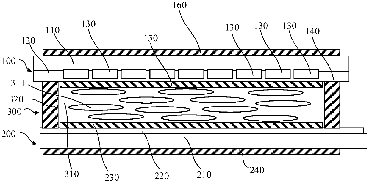
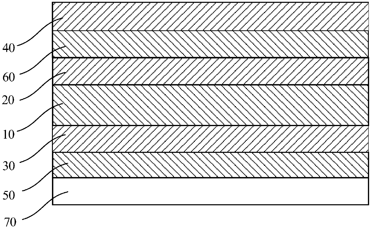
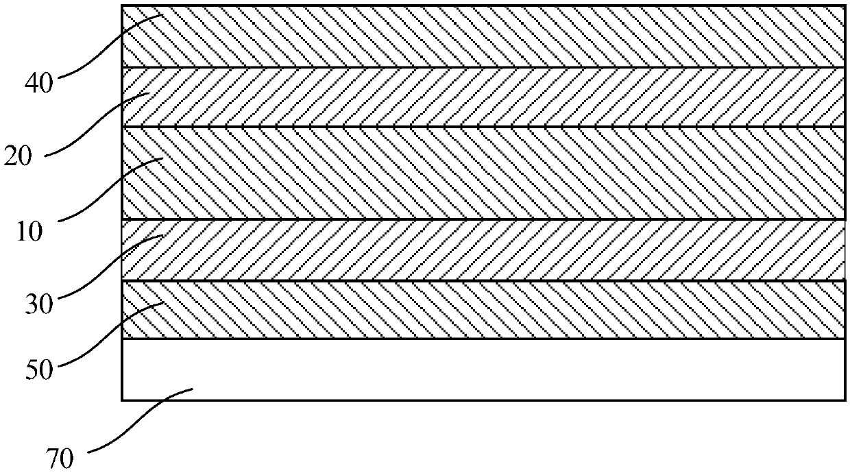
[0059] Such as Figure 1-Figure 3 As shown, this embodiment discloses a display panel. The display panel can be used as a part of the display device. In addition to including the display panel, the display device may also include a housing. The interior of the casing is provided with a containing space for containing the display panel. The display device may also include elements such as sensors.

[0060] Such as figure 1 As shown, the display panel includes a first substrate 100 , a second substrate 200 and a display function unit 300 disposed between the first substrate 100 and the second substrate 200 . In this embodiment, the display function unit 300 includes a liquid crystal layer 310 and a sealing frame layer 320 . The first substrate 100 is a color filter substrate, the second substrate 200 is an array substrate, the first substrate 100 and the second substrate 200 are arranged in pairs, and the liquid crystal layer 310 and the sealing frame layer 320 are both arr...

Embodiment 2

[0080] Such as Figure 4 As shown, this embodiment discloses a display panel. The display panel of this embodiment is substantially the same as that of Embodiment 1, except that the display panel of this embodiment includes a base 410 and an organic light-emitting material disposed on the base 410. layer 420 , and the encapsulation layer 600 and polarizer 500 disposed on the organic luminescent material layer 420 , the organic luminescent material layer 420 serves as at least a part of the display functional unit. The display panel does not need a backlight. When current flows, the organic luminescent material layer 420 emits light, and the light emitted by the organic luminescent material layer 420 passes through the polarizer 500 and the encapsulation layer 600 to emit outwards.

[0081] Wherein, the encapsulation layer 600 is provided with a photosensitive material. Through the above settings, it is possible to automatically compensate the emitted light on the light-emitti...


PUM


Abstract

The invention discloses a display panel and a display device. The display panel comprises a plurality of pixel units, light-sensitive materials are arranged on the light-out sides of the pixel units,and the light-sensitive materials can change along with the intensity changes of light emitted by the pixel units to change the light transmission performance of the light-out sides where the light-sensitive materials are arranged. By means of the arrangement, a bright area, which is too high in brightness, of the display panel achieves dark compensation, a dark area which is too low in brightnessachieves bright compensation, so that automatic compensation for the emitted light is achieved, and the perception experience of a user is improved.

Description

technical field [0001] The invention relates to the display field, in particular to a display panel and a display device. Background technique [0002] Display devices with large size, high pixel density, and high charging efficiency are increasingly favored by users. However, in the manufacturing process, a thick copper process and an oxide process are required, resulting in a large-scale display device that cannot effectively compensate the brightness of light while pursuing high pixel density, and poor diffusion that cannot be recognized by the human eye often occurs. Moreover, when the product quality is displayed, there will be obvious uneven picture quality and poor gray scale, which will affect the user's perception experience. Contents of the invention [0003] Embodiments of the present invention provide a display panel and a display device, and the display panel and the display device can automatically compensate the brightness of light. [0004] According to t...

Claims


Application Information

Patent Timeline
IPC IPC(8): G02F1/1335G02F1/133
CPCG02F1/13318G02F1/133514G02F1/133528
Inventor 胡金良马健任文明
Owner HEFEI XINSHENG OPTOELECTRONICS TECH CO LTD
Why Eureka
Eureka Blog
Learn More