Method for preparing OLED device

A device and process technology, applied in the field of light-emitting display, can solve problems such as poor film thickness uniformity, and achieve the effect of uniform film thickness distribution

Active Publication Date: 2019-04-26
SHENZHEN CHINA STAR OPTOELECTRONICS SEMICON DISPLAY TECH CO LTD
View PDF5 Cites 0 Cited by
  • Summary
  • Abstract
  • Description
  • Claims
  • Application Information

AI Technical Summary

Problems solved by technology

[0010] The reason for the uneven film thickness is mainly that in the IJP process, the printed solvent itself volatilizes non-uniformly to the surroundings, thus due to the influence of the steam when the solvent in the printing ink volatilizes, it will cause the display The thickness uniformity of the s-pixel intima in the outermost row and column of the area is poor, and it appears concentrated to one side

Method used


Image

  • Method for preparing OLED device
  • Method for preparing OLED device

Examples


Embodiment Construction

[0035] The technical scheme of a method for manufacturing an OLED device involved in the present invention will be described in further detail below with reference to the accompanying drawings and embodiments.

[0036] One embodiment of the present invention provides a method for preparing an OLED device, comprising the following steps:

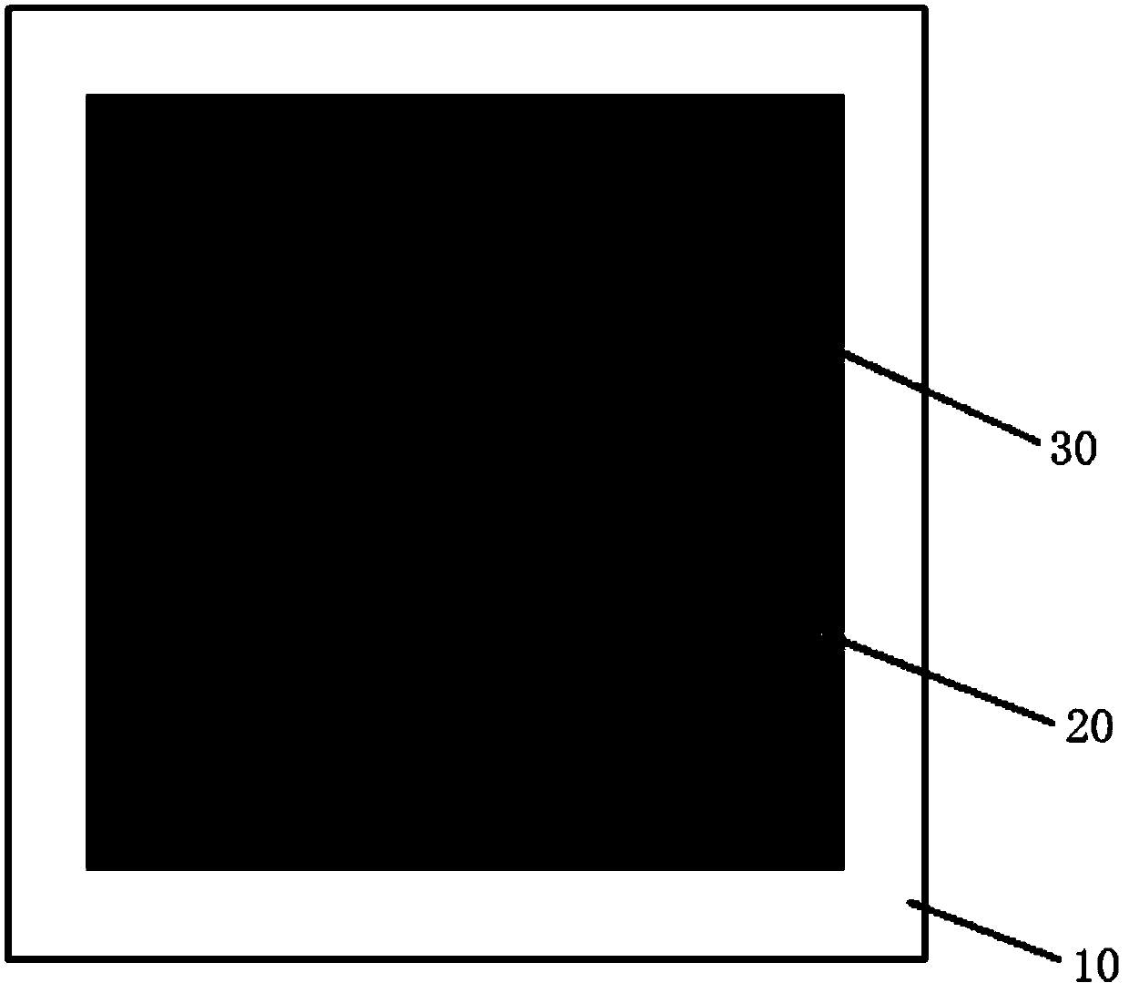
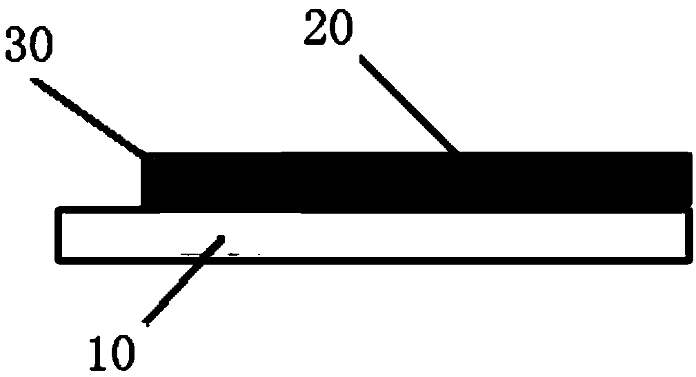
[0037] providing a substrate on which a display area is defined and a temporary coating area located outside the edge of the display area, wherein the temporary coating area is disposed adjacent to the edge of the display area and surrounds the display area;

[0038] The prepared volatile organic resin is coated on the temporary coating area by coating to form a dummy area, and the width of the temporary coating area on each side of the display area is between 2 mm and 100 mm. For example, 15mm, 20mm, 30mm, 50mm, 60mm, etc., the details can be determined according to the needs, and there is no limit;

[0039] Coating a blank solvent of print...


PUM


Abstract

The invention provides a method for preparing an OLED device. The method comprises the following steps of providing a substrate, defining a display area and a temporary coating area (dummy area) outside the edge of the display area on the substrate, wherein the temporary coating area is disposed adjacent to the edge of the display area; preparing a device structure in the display area through a solvent method on the substrate and coating a first solvent on the temporary coating area; removing the first solvent coated on the temporary coating area. According to the method for preparing the OLEDdevice, an additional evaporation area is arranged to offset the impact of the solvent on the edge s-pixel of the display area of the device during evaporation, so that uniform thickness distributionof the film thickness in s-pixel on rows and lines on the edge of the display area can be effectively ensured.

Description

technical field [0001] The invention relates to the technical field of light-emitting display, in particular, a method for preparing an OLED device. Background technique [0002] It is known that the organic electroluminescent device (OLED) has become the most promising new display device in recent years due to its advantages of self-luminescence, all-solid-state, high contrast and the like. [0003] Further, the use of evaporation equipment to prepare OLED devices is currently the mainstream method of production in the industry. However, this evaporation process has disadvantages such as low material utilization rate and poor uniformity, and the industry has always lacked an effective solution for this. However, the solution method developed later to prepare OLED thin films has gradually shown its advantages due to its high material utilization rate and low equipment cost. [0004] The solution process mainly includes methods such as spin coating, printing, and printing. ...

Claims


Application Information

Patent Timeline
Patent Type & Authority Applications(China)
IPC IPC(8): H01L51/56
CPCH10K71/12
Inventor 郝鹏
Owner SHENZHEN CHINA STAR OPTOELECTRONICS SEMICON DISPLAY TECH CO LTD
Why Eureka
Try Eureka