Schottky clamped SCR device for ESD protection
A Schottky contact and Schottky diode technology, applied in electronic science and field, to achieve the effect of improving anti-latch capability
- Summary
- Abstract
- Description
- Claims
- Application Information
AI Technical Summary
Problems solved by technology
Method used
Image
Examples
Embodiment 1
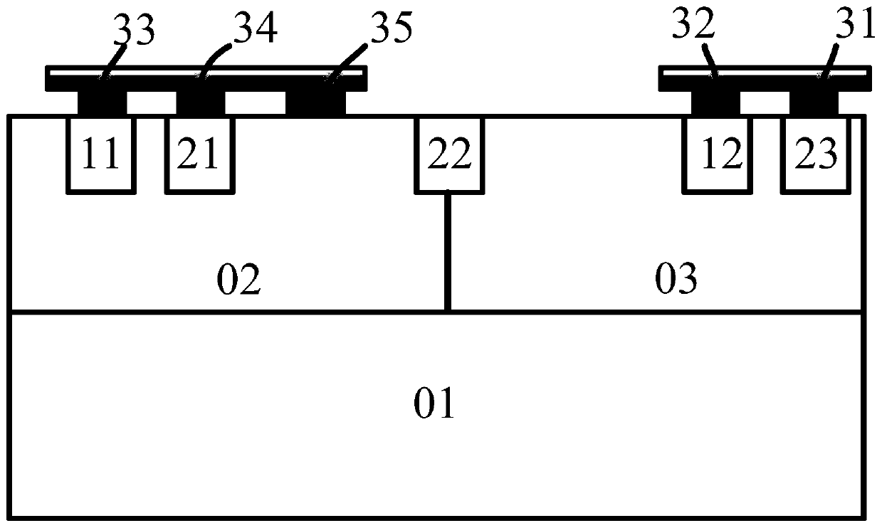
[0023] Such as image 3 As shown, a Schottky clamp SCR device for ESD protection includes: P-type substrate 01, p-well region 02 and n-well region 03 above P-type substrate 01, and p-well region 02 and n-well region The well region 03 is tangent, the first n+ injection layer 21 and the first p+ injection layer 11 inside the p well region 02, the third n+ injection layer 23 and the second p+ injection layer 12 inside the n well region 03, bridged The second n+ injection layer 22 used to reduce the breakdown voltage between the n well region 03 and the p well region 02, the first metal hole 31 is in contact with the third n+ injection layer 23, the second metal hole 32 is in contact with the second The p+ injection layer 12 is in contact, the third metal hole 33 is in contact with the first p+ injection layer 11, the fourth metal hole 34 is in contact with the first n+ injection layer 21, and the fifth metal hole 35 is directly in contact with the p well region 02 A Schottky co...
Embodiment 2
[0030] Such as Figure 6 Shown: the operating principle of this embodiment is the same as that of embodiment 1. The difference is that the fifth metal hole 35 in Embodiment 1 is removed, and a new sixth metal hole 36 is made on the left side of the second metal hole 32 to contact the n-well region 03 to form an N-type Schottky diode 104 .
[0031] In the equivalent circuit as Figure 7 As shown, an N-type Schottky diode 104 is connected in parallel to the emitter junction of the PNP transistor 101 . Its scope of work and principle are identical with embodiment 1.
Embodiment 3
[0033] Such as Figure 8 Shown: the operating principle of this embodiment is the same as that of embodiment 1. The difference is that the fifth metal hole 35 in Embodiment 1 is retained, and a new sixth metal hole 36 is made on the left side of the second metal hole 32 to contact the n-well region 03 to form a Schottky diode. reflected in the equivalent circuit as Figure 9 As shown, an N-type Schottky diode 104 is connected in parallel to the emitter junction of the PNP transistor 101 . A P-type Schottky diode 103 is connected in parallel to the emitter junction of the NPN transistor 102 . Its working scope and principle are the same as those of Embodiment 1.
[0034]In summary, the present invention proposes a Schottky clamp SCR structure for ESD protection. Due to the fact that the additional Schottky diode has a certain inhibitory effect on the positive feedback effect of the SCR, the maintenance voltage rises when the SCR is turned on to discharge the ESD current, so...
PUM
 Abstract
Description
Claims
Application Information


