
Eureka
For R&D, Eureka makes reading and utilizing patents & technical documents easy.
Eureka AIR
Designed for self-driven R&D workflows. Generate viable solutions, solve complex R&D challenges, empower your innovation with AI.

Eureka Materials
Designed for material experts only. Revolutionize your material R&D, from search, analyze, to developing new materials.

TechResearch
Generate reliable direction feasibility study reports for your R&D in just a few steps.

TechSeek
Discover and master advanced knowledge NOW. Basics, ideas, possibilities, all at once.

TechMind
As an expert in R&D Theories, TechMind can generates customized viable solutions instantly.

TechRisk
Analyze your overall solution with one click, know your potential R&D risks in advance.

TechMonitor
Get weekly tech updates, stay abreast of the latest tech innovations and key insights.
A packaging substrate, a semiconductor device and a manufacturing method of the semiconductor device
A technology for encapsulating substrates and manufacturing methods, which is applied to semiconductor devices, electrical solid devices, electrical components, etc., can solve the problems of short service life of semiconductor devices, poor thermal conductivity of white glue, and inability to dissipate in time, so as to prolong the service life, Avoid cracking, avoid the effect of white glue cracking
- Summary
- Abstract
- Description
- Claims
- Application Information
AI Technical Summary
Problems solved by technology
Method used
Image

Examples
Embodiment Construction
[0036] In the following description, numerous specific details are set forth in order to provide a thorough understanding of the present invention. However, the present invention can be implemented in many other ways different from this description, and those skilled in the art can make similar extensions without violating the connotation of the present invention, so the present invention is not limited by the specific embodiments disclosed below.
[0037] The technical solution of the present invention will be clearly and completely described below in combination with specific embodiments and accompanying drawings.
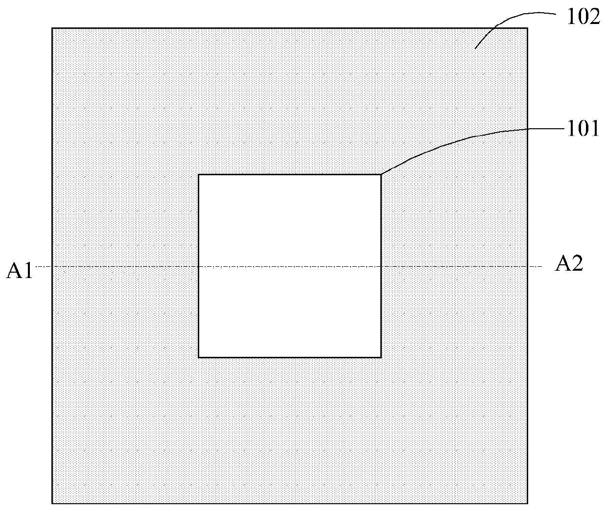
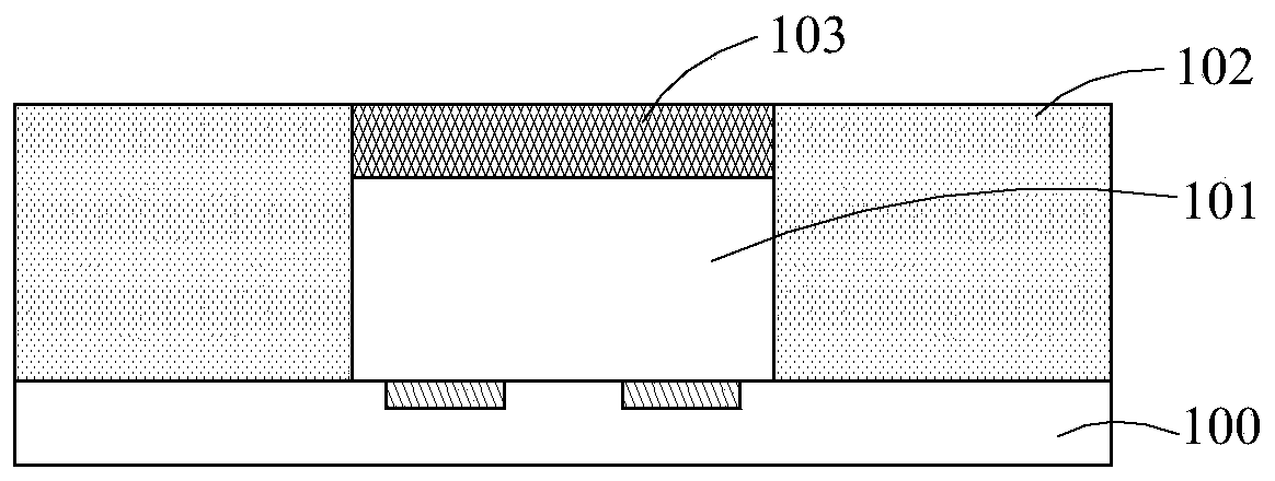
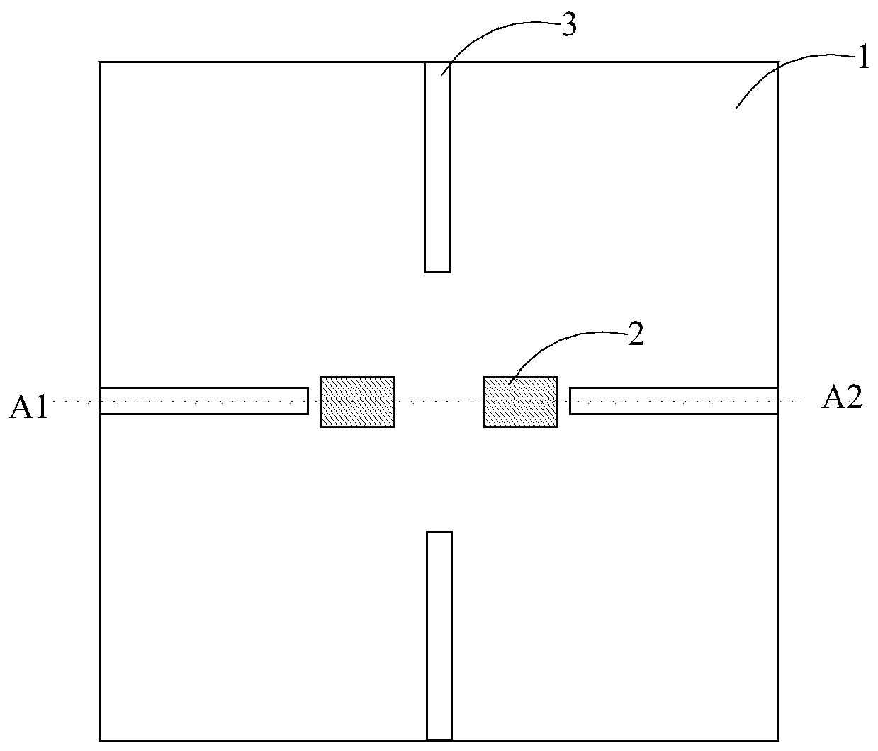
[0038] See image 3 , is a structural schematic diagram of an embodiment of a packaging substrate of the present invention.
[0039] Such as image 3 As shown, the packaging substrate includes: a substrate 1, an electrode 2 and several heat sinks 3; the electrodes 2 and the several heat sinks 3 are arranged on the upper surface of the substrate 1, and the sever...
PUM
 Abstract
Description
Claims
Application Information
 - R&D Engineer
- R&D Manager
- IP Professional
- Industry Leading Data Capabilities
- Powerful AI technology
- Patent DNA Extraction
Browse by: Latest US Patents, China's latest patents, Technical Efficacy Thesaurus, Application Domain, Technology Topic, Popular Technical Reports.
© 2024 PatSnap. All rights reserved.Legal|Privacy policy|Modern Slavery Act Transparency Statement|Sitemap|About US| Contact US: help@patsnap.com