

Memory and formation method thereof
A memory and storage area technology, applied in the direction of electric solid-state devices, semiconductor devices, electrical components, etc., can solve the problems of complex process and low production efficiency, and achieve the effect of simplifying and reducing the process flow
- Summary
- Abstract
- Description
- Claims
- Application Information
AI Technical Summary
Problems solved by technology
Method used
Image

Examples
Embodiment Construction
[0027] As mentioned in the background, prior art memories have poor performance.
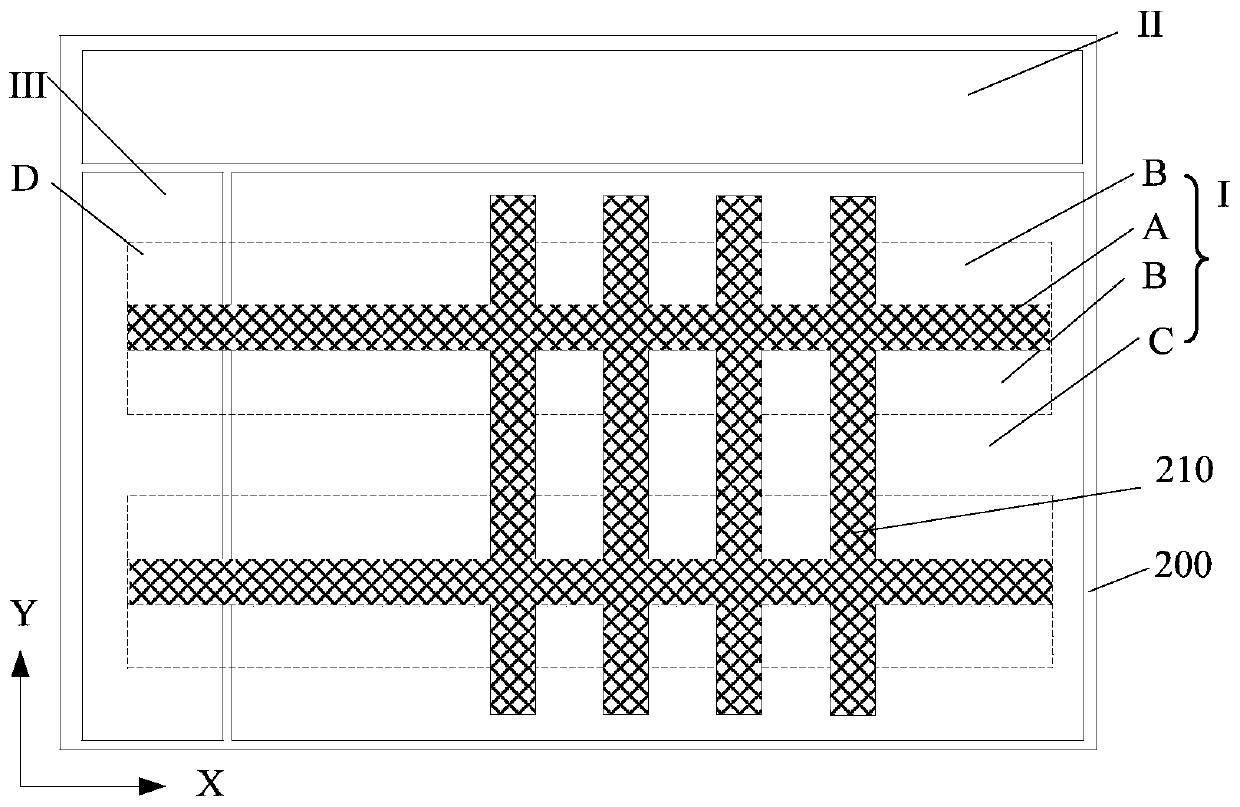
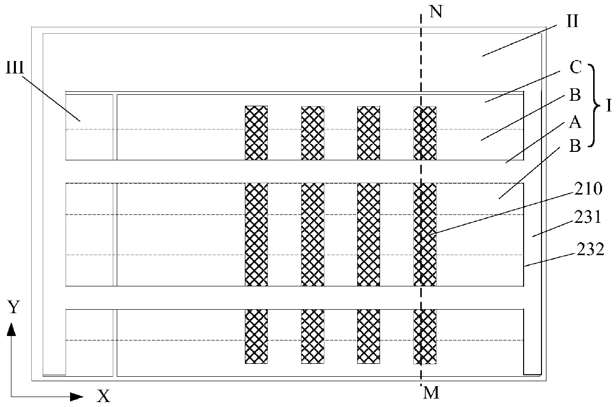
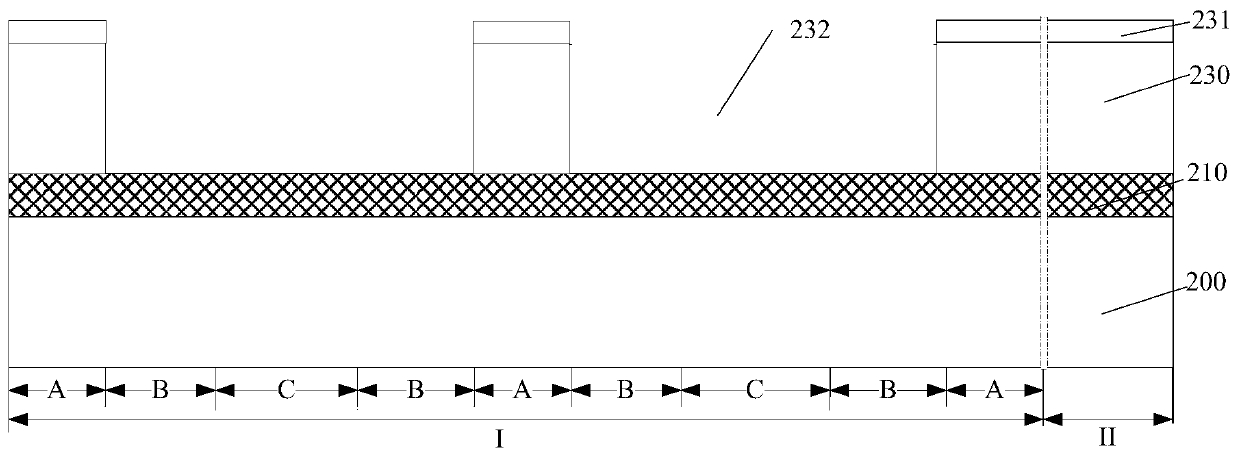
[0028] A memory, comprising: a substrate, the substrate includes an erasing area and a floating gate area, the floating gate area is adjacent to the erasing area and located on both sides of the erasing area; In addition to the gate structure; the floating gate structure respectively located on the floating gate region of the substrate; the first side wall, the second side wall and the control gate structure located on the floating gate structure, the second side wall is located on the control gate structure On the gate structure, the first sidewall is parallel to the second sidewall and the control gate structure.
[0029] In the formation process of the above-mentioned memory, one mask is required to form the erasing gate structure, the control gate structure and the floating gate structure, so at least three patterning processes are required. When continuing to form the word line structure c...
PUM
 Abstract
Description
Claims
Application Information