A chip data processing method and system based on an AES-GCM

A data processing system and data processing technology, applied in the direction of encryption device with shift register/memory, etc., can solve the problems of large chip area overhead and delay, increased data processing delay, consumption-level combinational logic, etc. The effect of chip area, reducing latency, solving timing problems

Inactive Publication Date: 2019-05-03
SUZHOU CENTEC COMM CO LTD
View PDF3 Cites 3 Cited by
  • Summary
  • Abstract
  • Description
  • Claims
  • Application Information

AI Technical Summary

Problems solved by technology

[0005] In the existing technology, the H power operation is started after the chip is powered on and initialized. After the operation is completed, it is sent to the encryption and decryption engine for encryption or decryption operations. Since the H power budget requires a lot of AND and XOR logic, this stage requires many levels of combinatorial logic, and there will be timing issues
To solve the timing problem, it is necessary to increase the flip-flop, which leads to an increase in the delay of data processing and increases the chip area.
For example, if the data bit width is 200 bytes, 1600 flip-flops need to be added for each additional level of pipeline. The more flip-flops are added, the greater the area overhead and delay of the chip.

Method used


Image

  • A chip data processing method and system based on an AES-GCM
  • A chip data processing method and system based on an AES-GCM
  • A chip data processing method and system based on an AES-GCM

Examples


Embodiment Construction

[0041] In order to enable those skilled in the art to better understand the technical solutions in the present invention, the technical solutions in the embodiments of the present invention will be clearly and completely described below in conjunction with the drawings in the embodiments of the present invention. Obviously, the described The embodiments are only some of the embodiments of the present invention, not all of them. Based on the embodiments of the present invention, all other embodiments obtained by persons of ordinary skill in the art without making creative efforts shall fall within the protection scope of the present invention.

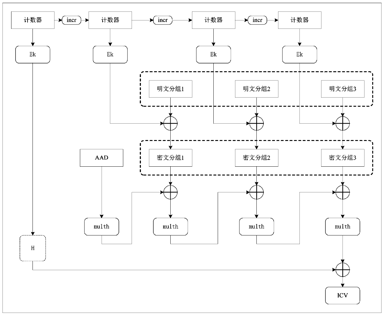
[0042] ginseng Figure 5 As shown, the present invention discloses a chip data processing method based on AES-GCM, comprising:

[0043] S1. Initialize the chip;

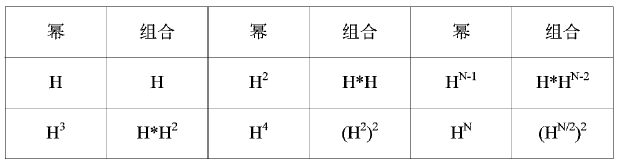
[0044] S2. Use the key k to perform AES encryption on the binary number "0" to obtain the variable H, and calculate the integer power of the variable H;

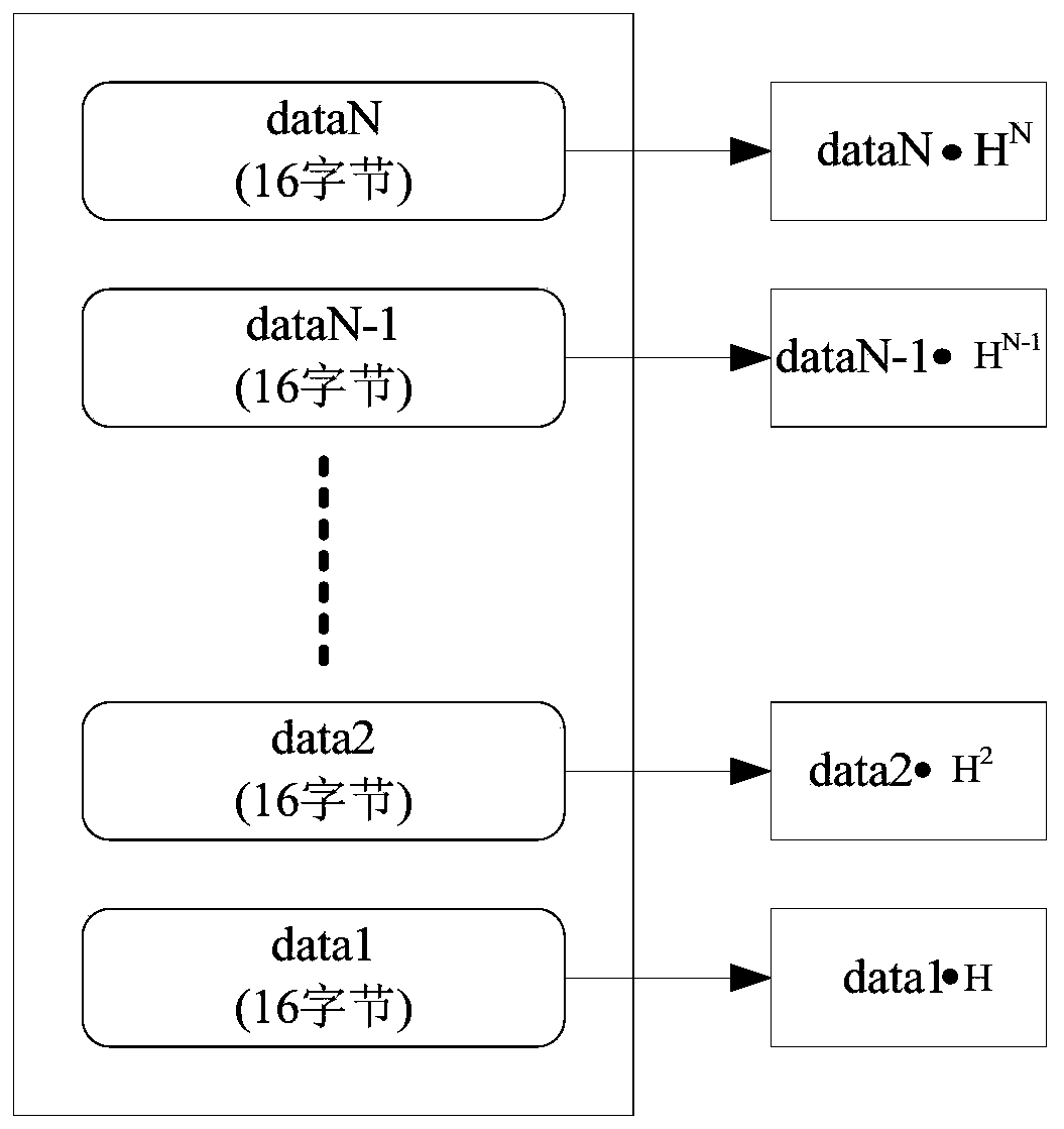
[0045]S3. Based o...


PUM


Abstract

The invention provides a chip data processing method and system based on an AES-GCM. The method comprises the steps that S1, initializing a chip; S2, performing AES encryption on the binary number '0'by using a key k to obtain a variable H, and calculating the integer power of the variable H; And S3, grouping the plaintext data based on an AES algorithm, carrying out point multiplication on eachgroup of plaintext data and the integer power of the corresponding variable H in a finite field, and finally obtaining the ICV value of the authentication tag. According to the invention, the delay ofdata processing is reduced, the operation speed of the chip is improved, the number of triggers is reduced, and the area of the chip is reduced.

Description

technical field [0001] The invention relates to the technical field of chip information security, in particular to an AES-GCM-based chip data processing method and system. Background technique [0002] The GCM algorithm (Galois / Counter Mode, using Counter mode for symmetric encryption, and with ICV message authentication code) can provide encryption and integrity verification of messages, and can provide integrity verification of additional authentication data. In practical applications In the scenario, some information does not need to be kept secret, but the receiver of the information needs to confirm its authenticity, such as source port, destination port, IV, etc. Therefore, this part of data needs to be added to the calculation of the ICV value (IntegrityCheck Value, authentication label) as additional authentication data. The AES algorithm (Advanced Encryption Standard, Advanced Data Encryption Standard) is a symmetric block cipher algorithm widely used in the field ...

Claims


Application Information

Patent Timeline
Patent Type & Authority Applications(China)
IPC IPC(8): H04L9/06
Inventor 孙冠男龚源泉夏杰
Owner SUZHOU CENTEC COMM CO LTD
Why Eureka
Try Eureka